
Professional PCB manufacturing and assembly
Building 6, Zone 3, Yuekang Road,Bao'an District, Shenzhen, China
+86-13410863085Mon.-Sat.08:00-20:00

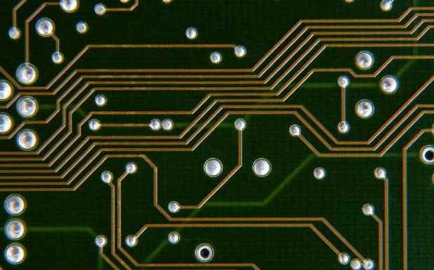
What is a differential signal? In plain English, the driver sends two equivalent, inverting signals, and the receiver determines whether the logical state is "0" or "1" by comparing the difference between the two voltages. The pair carrying the differential signal is called differential routing.
Compared with ordinary single-ended signal routing, differential signal has the most obvious advantages in the following three aspects:
a. Strong anti-interference ability, because the coupling between the two differential wires is very good, when there is noise interference from the outside, it is almost coupled to the two lines at the same time, and the receiver only cares about the difference between the two signals, so the common mode noise from the outside can be completely cancelled out.
b. can effectively inhibit EMI. Similarly, because the polarity of two signals is opposite, the electromagnetic fields radiated by them can cancel each other. The closer the coupling, the less electromagnetic energy released to the outside world.
c. Precise timing positioning. Since the switching change of differential signal is located at the intersection of two signals, unlike ordinary single-ended signal which depends on the high and low threshold voltage, it is less affected by technology and temperature, which can reduce the error in timing and is more suitable for the circuit with low amplitude signal. LVDS (low voltage differential signaling), which is popular at present, refers to this small amplitude differential signaling technology.

For PCB engineers, the most important thing is to ensure that the advantages of differential routing can be fully utilized in the actual routing. Perhaps as long as the contact with Layout people will understand the general requirements of differential routing, that is, "equal length, equal distance". The equal length is to ensure that the two differential signals maintain opposite polarity at all times and reduce the common-mode component. Equidistance is mainly to ensure that the difference impedance is consistent and reduce reflection. "As close as possible" is sometimes a requirement for differential routing. But none of these rules are meant to be copied, and many engineers seem unaware of the nature of high-speed differential signal transmission. Several common errors in PCB differential signal design are discussed below.
Misconception 1: believe that differential signals do not need ground plane as a backflow path, or think that differential routes provide backflow paths for each other. The reason for this misunderstanding is that the surface phenomenon is confused, or the mechanism of high-speed signal transmission is not deep enough. As can be seen from the structure of the receiving end of FIG. 1-8-15, the emitter currents of transistors Q3 and Q4 are equivalent and opposite. Their currents at the junction exactly cancel each other out (I1=0), so the differential circuit is insensitive to similar bombs and other noise signals that may exist on the power supply and ground plane. Partial backflow cancellation in the ground plane does not mean that the differential circuit does not take the reference plane as the signal return path. In fact, in the analysis of signal backflow, the mechanism of differential routing is the same as that of ordinary single-ended routing, that is, high-frequency signals always carry out backflow along the loop with the smallest inductance. The biggest difference lies in that the difference lines are coupled to the ground as well as to each other. Whichever coupling is strong becomes the main backflow path. FIG. 1-8-16 shows the distribution diagram of the geomagnetic field of single-ended signal and differential signal.
In PCB circuit design, the coupling between differential routing is generally small, often accounting for only 10~20% of the coupling degree, more or the coupling to the ground, so the main return path of differential routing still exists in the ground plane. When discontinuity occurs in the ground plane, the coupling between differential routes will provide the main return path in the area without reference plane, as shown in FIG. 1-8-17. Although the impact of the discontinuity of the reference plane on the differential routing is not as serious as that on the ordinary single-ended routing, it will still reduce the quality of the differential signal and increase EMI, which should be avoided as far as possible. Some designers believe that the reference plane of the differential line can be removed to suppress part of the common-mode signal in the differential transmission, but this is not desirable theoretically. How to control the impedance? Not providing ground impedance circuit for common-mode signal will inevitably cause EMI radiation, which does more harm than good.
Myth 2: Maintaining equal spacing is more important than matching line length. In the actual PCB routing, the requirements of differential design can not be met at the same time. Due to the pin distribution, through hole, and routing space and other factors, it is necessary to achieve the purpose of line length matching through appropriate winding, but the result must be that part of the difference pair cannot be parallel. At this time, how should we choose? Before jumping to conclusions let's take a look at the following simulation results.


Just upload Gerber files, BOM files and design files, and the KINGFORD team will provide a complete quotation within 24h.