
Professional PCB manufacturing and assembly
Building 6, Zone 3, Yuekang Road,Bao'an District, Shenzhen, China
+86-13410863085Mon.-Sat.08:00-20:00


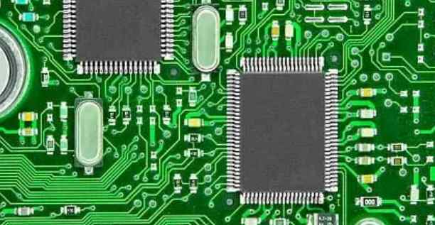
In the maintenance of pcb circuit board, it is a headache to encounter the short circuit of VCC power supply, because there are too many components in parallel between VCC and GND, such as chips, capacitors and transistors, which may short circuit, tin point and copper foil may short circuit. Generally, the components are removed one by one until the short circuit is removed after the removal of a component. If bad luck, the components on the whole board are almost removed and can not find the fault, not only can not find the fault, but also the circuit board will be damaged. Cut the circuit board copper foil, this is also very difficult.
In this pcb circuit board manufacturer introduces two more convenient methods:
1, for the plug-in capacitor on the circuit board can use diagonal pliers to cut a foot (pay attention to cut from the middle, do not cut root or circuit board cut), plug-in IC can cut the power supply VCC foot, when a short circuit disappears when cutting a foot, then a chip or capacitor short circuit. If it is a patch IC, the power pin of the IC can be lifted after melting the solder with an electric iron, so that it leaves the VCC power supply. After replacing the short circuit element, weld the cut or warped part again.

2. There is a faster method, but it requires a special meter ---- milliohm. As we all know, the copper foil on the circuit board also has resistance. If the copper foil thickness on the PCB is 35um and the printed wire width is 1mm, the resistance value is about 5mΩ for every 10mm length. Such a small resistance value can not be measured by ordinary multimeters, but can be measured by milliohm meters. It can be assumed that a component is short circuit, measured by an ordinary multimeter is 0Ω, measured by a milliohm meter may be tens of milliohm to hundreds of milliohm, the pen is just placed on the short circuit element two feet measurement, the resistance value obtained must be minimum (because if placed on the other components two feet measurement, the resistance value also includes the copper foil on the circuit board resistance), In this way, by comparing the resistance difference of the milliohm meter, when a component is measured (if it is a solder or copper foil short circuit is the same reason) to get the lowest resistance value, then the component is the key suspect object. In this way, the fault can be found quickly.
PCB circuit board analysis of PCB wiring six points for attention
First, when designing the printed circuit board of the logic circuit, the ground wire should form a closed-loop form, which can effectively improve the anti-interference ability of the circuit.
Two, the ground wire should be as thick as possible. As we all know, the resistance of the thin wire is larger. If the resistance is larger, the ground potential will change with the change of the current, which will lead to the instability of the signal level, and thus the decrease of the anti-interference ability of the circuit.
Three, pay attention to the choice of ground point. When the signal frequency on the circuit board is lower than 1MHz, because the electromagnetic induction effect between wiring and components is small, and the circulation formed by the grounding circuit has a greater impact on the interference, so it should be used to ground a little, so that it does not form a loop. When the signal frequency on the circuit board is higher than 10MHz, the grounding impedance becomes large due to the obvious inductance effect of the wiring. At this time, the circulation formed by the grounding circuit is no longer the main problem. Therefore, multi-point grounding should be used to reduce the ground impedance as far as possible.
Four, the layout of the power line in addition to according to the size of the current as far as possible to thicken the width of the wire, in the wiring should also make the power line, ground wire direction and data line of the line body in the wiring work at the end, the ground line will be the bottom of the circuit board without the line covered, these methods are helpful to enhance the anti-interference ability of the circuit.
Five, the width of the data line should be as wide as possible to reduce the impedance.
Vi. The number of holes should be reduced as far as possible. It should be known that a hole in the circuit board will bring about 10pF capacitance effect, which is a great interference in high-frequency circuits, so it is necessary to reduce the number of holes as much as possible, in addition, too many holes will cause the mechanical strength of the circuit board will be greatly weakened.


Just upload Gerber files, BOM files and design files, and the KINGFORD team will provide a complete quotation within 24h.