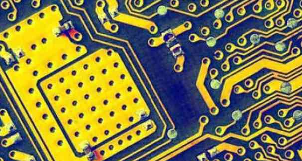
With the development of electronic products in the direction of "light, thin, short and small", PCB also develops to high density and high difficulty, so a large number of SMT and BGA PCB appear, and customers require plug holes when pasting components. After a lot of practice, the traditional aluminum plug process is changed, and white mesh is used to complete the circuit board surface welding and plug holes. Stable production and reliable quality.
Why plug the PCB board through the hole?
The Via hole plays the role of connecting the lines to each other. The development of the electronics industry also promotes the development of PCB, which also puts forward higher requirements for the production process and surface mounting technology of printed board. Via hole plugging technology comes into being and should meet the following requirements:
(1) There is copper in the through hole, and welding resistance can be plugged or not plugged;
(two) there must be tin lead in the through hole, there is a certain thickness requirement (4 microns), no solder resistance ink into the hole, resulting in tin beads in the hole;
(three) the pass-through hole must have solder resistance ink plug hole, light proof, no tin ring, tin beads and flat requirements.
With the development of electronic products to the direction of "light, thin, short, small", PCB also to high density, high difficulty development, so there are a large number of SMT, BGA PCB, and customers require plug holes when pasting components, mainly has five functions:
(a) To prevent PCB over wave soldering tin through the through hole through the component surface resulting in short circuit; In particular, when we put the hole on the BGA pad, we must first do the plug hole, and then gold-plated treatment, to facilitate the welding of BGA.
(2) To avoid flux residue in the pass-through hole;
(3) After the completion of surface mounting and component assembly in the electronics factory, the PCB should be vacuated on the testing machine to form negative pressure:
(four) prevent the surface solder paste into the hole caused by virtual welding, affecting the installation;
(5) To prevent over wave soldering tin bead pop out, resulting in short circuit.
The realization of conductive hole plugging process
For the surface mounting plate, especially the mounting of BGA and IC, the requirements for the through-hole plug hole must be flat, convex and concave plus or minus 1mil, and the edge of the through-hole shall not be red and tinned; Through the hole hidden tin beads, in order to meet customer requirements, through the hole plugging process is all over the place, the process is particularly long, process control is difficult, often in hot air leveling and green oil soldering resistance experiment oil loss; Problems such as oil explosion occur after curing. Now according to the actual conditions of production, the PCB plug process is summarized, in the process and advantages and disadvantages of some comparison and elaboration:
Note: The working principle of hot air smoothing is to use hot air to remove excess solder on the surface of the printed circuit board and inside the hole, and the remaining solder is uniformly covered on the welding plate and the line and surface seal decoration of the open solder, which is one of the surface treatment methods of the printed circuit board.

First, hot air leveling after plugging process
The process flow is: plate welding resistance →HAL→ plug → curing. Non-plug hole process is used for production. After hot air leveling, aluminum sheet screen or ink screen is used to complete the through-hole plug holes of all strongholds required by customers. Plug hole ink can be photosensitive ink or thermosetting ink, in order to ensure that the wet film color is consistent, plug hole ink is best used with the same ink. This process can ensure that the hot air leveling through the hole does not drop oil, but easy to cause plug hole ink pollution, uneven surface. It is easy for customers to cause virtual welding when mounting (especially in BGA). So many customers don't accept this approach.
Two, hot air leveling before plugging process
2.1 Pattern transfer is carried out with aluminum sheet after plugging, curing and grinding
This process uses a CNC drilling machine to drill out the aluminum sheet to plug holes, make a screen version, plug holes, to ensure that the through hole plug hole full, plug hole ink, plug hole ink can also be used thermosetting ink, its characteristics must be high hardness, small resin shrinkage change, and hole wall binding force. The process flow is as follows: pretreatment → plug → grinding → pattern transfer → etching → plate resistance welding.
This method can ensure that the plug hole of the conduction hole is smooth, and there will be no quality problems such as oil explosion and hole edge oil in hot air leveling. However, this process requires one-time thickening of copper, so that the copper thickness of the hole wall can meet the customer's standard. Therefore, it has high requirements on the copper plating of the whole plate and the performance of the grinding machine, so as to ensure that the resin on the copper surface is completely removed, and the copper surface is clean and not polluted. Many PCB factories do not have one-time copper thickening process, and the performance of the equipment can not meet the requirements, resulting in this process is not used much in PCB factories.


