
Professional PCB manufacturing and assembly
Building 6, Zone 3, Yuekang Road,Bao'an District, Shenzhen, China
+86-13410863085Mon.-Sat.08:00-20:00

As PCB board design continues to grow, the PCB industry begins to accelerate year by year. Since the inception of HDI PCBS, the use of high density interconnects has changed the traditional structure of PCBS. HDI PCBS are a newer technology that allows PCBS to be built with smaller feature sizes and a lower cost process. These advantages make HDI the most common interconnect technology in advanced PCBS today. However, despite its popularity, there is still some confusion about what an HDI pcb is and what it can do.
This guide aims to introduce you to some of the major differences between other PCB technologies and how HDI PCBS are best for you.
What are HDI PCBS: The Basics
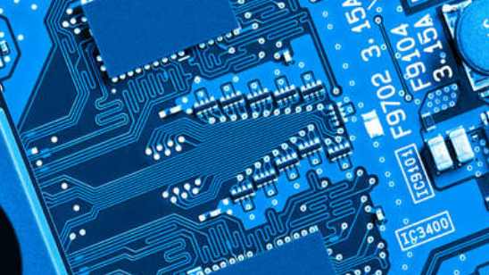
HDI PCBS stand for high density interconnection, which means multiple copper layers are built into a single board. This allows engineers to create boards that are thinner than traditional multilayer designs.
The main benefit of using HDI pcb boards is that they allow you to design smaller products while ensuring that your circuit gets the power it needs. They can also more easily route signals between different parts of the circuit without having to go through more important routing or through-holes. It is ideal for space-saving applications that need to consider thickness but still want the performance advantage of thicker boards.

HDI PCBS and Traditional PCBS: Manufacturing
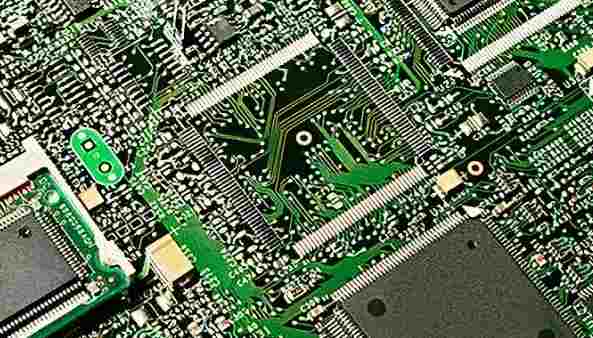
The main difference between traditional multilayer panels and HDI panels is their manufacturing process. Traditional multilayer PCBS are made by placing copper foil on both sides of the substrate and then using an etching process to remove a thin layer of copper from the top. After removing the copper, the trace is added to the remaining substrate material. HDI pcb boards, on the other hand, use a different process where a thin layer of copper is placed on one side of the substrate and etched away, leaving space between the trace lines on both sides of the board. This means that HDI pcb boards have characteristics that traditional multilayer boards do not have, such as through hole (THV), blind hole (BV), buried hole (BV), etc.
What's different about HDI PCBS?
Here are some of the advantages of HDI PCBS over standard PCBS, showing how they differ from other types of PCBS.
1. Improve thermal performance
By using copper foil instead of aluminum, HDI PCBS have better thermal performance than FR4. Copper is a better conductor of heat than aluminum and dissipates heat more efficiently than aluminum substrate. This reduces wasted power, which is especially important when dealing with high-power circuits such as motor drivers or power supplies.
2. Better signal integrity
HDI pcb boards can maintain signal integrity over longer distances than traditional single-layer boards because signal traces on different layers can be wired together more closely on the same plane. In addition, a signal trace on one layer can be routed over other traces on another layer without sacrificing signal quality due to capacitance effects.
3. Higher reliability
HDI PCBS improve system reliability by improving insulation between conductors and circuits, reducing crosstalk, and preventing short circuits between signals transmitted on adjacent planes. They also provide better mechanical strength by reducing stress concentration caused by a large number of tightly packed components.
4. Higher density
HDI pcb boards support more electrical connections per unit area than traditional single-layer boards. This is mainly due to the use of multiple layers as interconnects between layers in both laminated and blind holes.
5. It's smaller
Due to the increased wire density, the occupying area of HDI PCBS is smaller than traditional PCBS. This makes them ideal for portable electronics such as smartphones, tablets and laptops, as they require less space to fit all the components on a single board. The smaller size also makes them easier to produce on a single assembly line without having to create different tools for each product in different sizes.
6. Mechanical strength
HDI pcb boards can withstand greater pressure than standard PCBS. This is due to their design, which uses multiple layers of thin plastic bonded with an epoxy resin adhesive. The strength of each layer depends on the type of resin used in its structure.
7. Keep costs down
Because it is faster and cheaper to produce than a single panel, HDI pcb boards can be cheaper than other types of multilayer boards and other types of boards made of copper-clad panels (CCLS). They can be used for both small batch production runs and large batch production runs.
How to Use Flex PCB stiffener
May 11,2023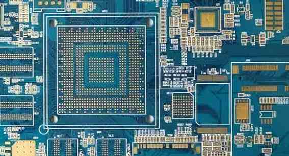


Just upload Gerber files, BOM files and design files, and the KINGFORD team will provide a complete quotation within 24h.