
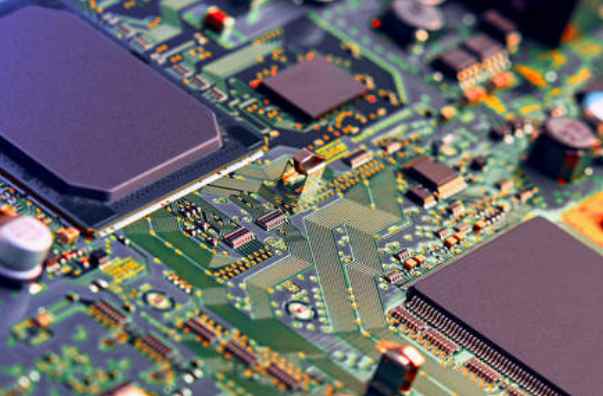
Professional PCB manufacturing and assembly
Building 6, Zone 3, Yuekang Road,Bao'an District, Shenzhen, China
+86-13410863085Mon.-Sat.08:00-20:00

Why is this theory and discussion of Maxwell's equations important for PCB designand layout? The answer is simple. We must first understand how electromagnetic fields are generated, and then we can reduce the electromagnetic fields generated by RF in PCBS. This has to do with reducing the RF current in the circuit. This RF current is directly related to the signal distribution network, bypass, and coupling. Radio-frequency currents eventually form harmonic frequencies and other digital signals.
The signal distribution network must be as small as possible in order to minimize the RF return current loop area. Bypass and coupling are related to the maximum current and must be transmitted through the power distribution network to generate a large current; The power distribution network, by definition, has a large area of RF return current loop.
The application of Maxwell equations
So far, the basic concepts of Maxwell's equations have been introduced. But how do you relate this knowledge of physics and advanced calculus to EMC in PCBS? For a thorough understanding, Maxwell's equation must be simplified again before it can be applied to PCB wiring. To apply it, we can relate Maxwell's equation to Ohm's law:
Ohm's law (time domain) : V = I * R
Ohm's Law (frequency domain) : Vrf= "Irf" * Z
V is the voltage, I is the current, R is the resistance, Z is the impedance (R + jX), rf is the radio frequency energy. If the RF current is present in the PCB circuit and the circuit has a fixed impedance value, an RF voltage will be generated and will be proportional to the RF current. Note that in the electromagnetic wave model, R is replaced by Z, which is a complex number with both resistance (real) and reactance (imaginary).
In terms of the impedance equation, there are many forms, depending on whether we want to look at the plane wave impedance, the circuit impedance... . Etc. For wire or PCB routing, the following formula can be used:

Cause and influence of emi in pcb
Where, XL=2πfL, is the only component in this formula related to the wire or PCB routing.
Xc=1/2(2πfC), omega =2πf
When the resistance value and inductance value of a component are known, such as: a "ferritebead-on-lead with wire", a resistor, a capacitor, or other devices with parasitic components, must consider the impedance size will be affected by the frequency, then the following formula can be applied:
When the frequency is greater than kHz, the reactance value is usually greater than R; But in some cases, that doesn't happen. The current will choose the path with the least impedance. When the number is lower than kHz, the path with the smallest impedance is the resistance. Above kHz, the path with the lowest reactance becomes dominant. At this point, because most circuits operate at frequencies above a few kHz, the idea that the current will choose the path with the least impedance becomes incorrect because it does not properly explain how the current flows in a transmission line.
For a wire carrying current frequency of more than 10 kHz, because its current always chooses the path with the least impedance, its impedance is equivalent to the path with the least reactance. If the load impedance is connected to a wire, cable, or wire and is greater than the capacitance in parallel with it on the transmission line path, the inductance becomes dominant. If all connected wires have roughly the same cross-sectional area, the path with the smallest inductance is the path with the smallest loop area. The smaller the loop area, the less inductance, and therefore, the current will flow to this path.
Each path has a finite impedance value. "Wire inductance" is the only reason why RF energy can be generated in PCBS. mounTIng pad welding wires may be too long, causing RF energy to exist. Winding a circuit board produces a very high inductance value, especially if the wire is to be wound for a long time. Long routes are those with long winding lengths, which result in a delay in the round-trip propagation of the signal in the route, and the next trigger signal is generated before it returns to the source driver (this is observed in the time domain). For observation in the frequency domain, refers to a long transmission line (line), its total length is about more than the frequency of λ/10, and this frequency exists in the transmission line (line). In simple terms, if an RF voltage is applied to an impedance, an RF current is obtained. It is this RF current that radiates RF energy into free space and thus violates EMC regulations. The above examples can help us understand Maxwell equations and PCB routing, and they are illustrated by very simple mathematical formulas.

Eliminate RF current in PCB
Mar 29,2023


Just upload Gerber files, BOM files and design files, and the KINGFORD team will provide a complete quotation within 24h.