
Professional PCB manufacturing and assembly
Building 6, Zone 3, Yuekang Road,Bao'an District, Shenzhen, China
+86-13410863085Mon.-Sat.08:00-20:00


In the era of industrialization surplus, circuit board manufacturers in particular, choose a suitable circuit board manufacturers is very important! In the industry, large companies such as Shennan, Shenlian and Jingwang are doing well. Their positioning is clear and their customer groups are very stable. Generally, they do not accept factory orders, because they are not short of orders at all.
However, most of the factories in the industry are not clearly positioned, what single is accepted, the result of what single is not good! Do not do well does not matter, reposition, do fine do special as a way out. But most of the boss don't think so, we think they pick up not only, because their strength is not enough, not enough equipment......
In fact, regardless of the size of the market, sometimes operating quality is more important than operating scale! PCB market is very big, you focus on a certain field, do fine, still can be bigger and stronger!
Shenzhen Fanyi Technology Development Co., Ltd. is such a circuit board company! We focus on connector RJ45Type C field for more than ten years, research RJ45 PCB board and Type C PCB board manufacturing difficulties, in 2007, there is no computer V-CUT period, can control the V-CUT tolerance within +/-0.15mm. When everyone thinks the single side welding ring ** meets 0.3mm, they have achieved 0.05mm!
Therefore, PCB proofing, production which good? Of course, choose Dongguan Qixiang Electronic Co., LTD., because Qixiang circuit has a team to study the inherent characteristics of each electronic industry products, according to the characteristics of different products, different production processes.
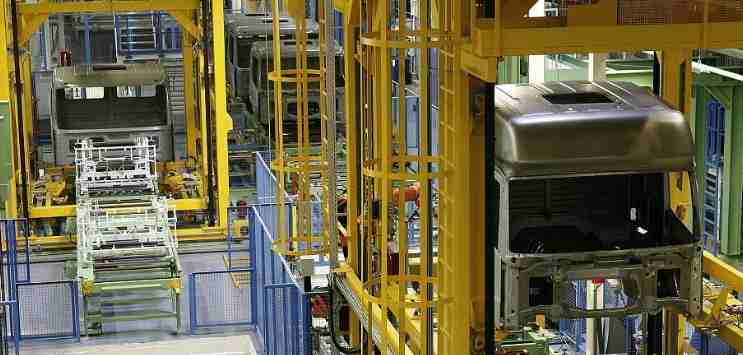
At present, there are too many circuit board factories and they are very miscellaneous. Electronic manufacturers to choose a wide range, and it is difficult to choose the right manufacturers. A little mistake, mismatched circuit board manufacturers will bring you a lot of annoyance, and even fatal functional problems, let you not hurt! Of course, the circuit board manufacturers are also many, such as Shennan, Shenlian, Jingwang these big factories, but the general large, circuit board factory is not just a factory, it is already a platform! It is not short of orders, will not choose to cooperate with you!

(1) Visual inspection Visual inspection is the use of human eyes to carry out some simple inspection, such as surface dents, pits, scratches, etc. * It is important to check whether the weld hole is in the center of the pad and the integrity of the wire pattern.
(2) Connectivity through holes For multi-layer circuit boards to conduct connectivity tests, the purpose is to find out whether the PCB graphics have connectivity.
(3) Insulation resistance of the circuit board Insulation resistance is a resistance of the printed circuit board insulation components to the external DC voltage. Choose two or more wires with close spacing and insulation, first measure the insulation resistance between them, after humidifying and heating for a period (the relative humidity in the box is about 45 degrees Celsius, 10 hours to two days), put them in the room for one hour, and then measure the insulation resistance between them.
(4) Weldability of welding pad Weldability is used to measure the wetting ability of solder on printed graphics when components are welded to the printed circuit board, which is generally expressed by wetting, semi-wetting and non-wetting. When wet, the solder can flow and expand freely on the wire and pad to form adhesive connection. Semi-wetting, the solder first wets the surface of the pad, and then forms the solder ball in some irregular places of the pad because of improper wetting. Without wetting, the solder accumulates on the surface, but does not form an adhesive connection to the pad surface.
(2) As a microelectronics IC learner, there is also a course in this semester: "Microelectronics devices", today I will talk about the basic devices: CMOS devices and circuits. We'll talk about latches and triggers later.
Today's main content is as follows:
· Brief introduction of MOS transistor structure and working principle
·CMOS unit circuit and layout
·CMOS gate circuit
· Power representation of CMOS
To be honest, CMOS is more micro electronic devices, micro electronic devices are really difficult... Here are a few things you might want to know about doing digital design (I'll add more later if necessary).
1. Brief introduction of structure and working principle of MOS transistor
It is more or less known that the main function of a transistor in a digital circuit is an electronic switch, which is turned on or off by a voltage or a current. There are roughly two kinds of transistors: One is bipolar junction transistor and the other is metal-oxide-semiconductor field-effect transistor (MOSFET or MOS). metal-oxide-semiconductor field effect transistor). Here we mainly talk about MOS, BJT in the current digital IC design is not the mainstream technology.
①MOS transistors are divided into PMOS and NMOS, which kind of MOS depends on the substrate and doping concentration. As for how it is formed, it is too complicated to explain in a few words, so let's skip it and look directly at their cross section diagram and briefly explain how they work (NMOS are taken as examples below).
The cross-sectional structure of the NMOS transistor is shown as follows:
IC design: CMOS devices and their circuits
The substrate is a silicon substrate (where the Body Si is), the top is a conductive gate, and the middle is an insulating layer composed of silica. In the past, the gate * was made of metal, so it was called metal-oxide-semiconductor. Now the gate * uses poly. In the MOS structure, a capacitor is formed by silica between a metal (polysilicon) and a semiconductor substrate.
Well, it doesn't matter if you don't understand the above paragraph, but remember that in the above NMOS transistor, the substrate is P-type, and there are two N-type doping regions on the substrate called Source and Drain. (You can define the left side as the drain and the right side as the source.) Since the device is symmetrical at this time, S and D are not really determined until the power supply and ground are connected), the upper middle is called Gate * (Gate), which is the three electrodes of NMOS (actually MOS is a 4-terminal device, and its substrate is also a terminal). Here's how they work.
Circuit board processing several times pressing
Mar 26,2023


Just upload Gerber files, BOM files and design files, and the KINGFORD team will provide a complete quotation within 24h.