
Professional PCB manufacturing and assembly
Building 6, Zone 3, Yuekang Road,Bao'an District, Shenzhen, China
+86-13410863085Mon.-Sat.08:00-20:00

In SMT chip processing, reflow soldering is a very important process. It is a welding process in which the SMT components are combined with the pads on the circuit board at high temperature and then cooled together, which has a great impact on the stability of the circuit board. It is also easy to have some process defects in reflow soldering, so it is necessary to analyze the causes and solve them accordingly to ensure product quality. The following quick technician mainly introduces the common defects and cause analysis of SMT reflow soldering.
1、 Tin bead
Reasons: 1. The silk screen hole is not aligned with the bonding pad, and the printing is inaccurate, which makes the solder paste dirty the PCB.
2. Solder paste is exposed too much in the oxidation environment and absorbs too much water in the air.
3. The heating is inaccurate, too slow and uneven.
4. The heating rate is too fast and the preheating interval is too long.
5. Solder paste dries too fast.
6. The activity of flux is not enough.
7. Too many small tin powders.
8. The volatility of flux is inappropriate during reflow.
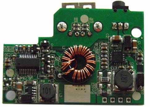
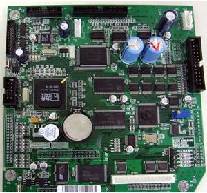
PCB proofing
2、 Open circuit
Reasons: 1. Insufficient solder paste.
2. The coplanarity of component pins is insufficient.
3. The tin is not wet enough (not melted enough, poor fluidity), and the solder paste is too thin, causing tin loss.
4. Solder absorption of pins (like rushes) or connecting holes nearby. Coplanarity of pins is particularly important for pin components with dense and ultra dense spacing. One solution is to tin the bonding pad in advance. Tin absorption of pins can be prevented by slowing down the heating speed and heating more at the bottom and less at the top.
3、 Solder crack
Reasons: 1. The peak temperature is too high, which makes the solder joint suddenly cool down. Due to the excessive thermal stress caused by chilling, solder cracks occur;
2. The quality of solder itself;
4、 Void
Reasons: 1. Material impact. Solder paste is damp, the oxygen content of metal powder in the solder paste is high, recycled solder paste is used, PCB component pin or PCB substrate pad is oxidized or polluted, and PCB is damp.
2. Influence of welding process: the preheating temperature is too low and the preheating time is too short, which makes the solvent in the solder paste fail to escape in time before hardening and enter the reflow zone to generate bubbles.
5、 Generally speaking, the factors that cause the tin bridge are that the solder paste is too thin, including low metal or solid content in the solder paste, low shake solubility, the solder paste is easy to be squeezed, the solder paste particles are too large, and the surface tension of the flux is too small. There is too much solder paste on the bonding pad, and the peak value of reflow temperature is too high.
SMT reflow soldering is a relatively complex process, which is easily affected by various factors. It is generally difficult to eliminate various defects. Understand the common defects of SMT reflow soldering and their causes, and pay more attention in the operation process to avoid defects. Once problems occur, they can be analyzed and solved in a timely manner.
Process of removing misprinted solder paste in SMT
As usual, paying attention to some details can eliminate undesirable situations, such as the misprint of solder paste and the removal of solidified solder paste from the board. It is our goal to deposit an appropriate amount of solder paste at the desired location. Dirty tools, dried solder pastes, and misalignment between templates and plates may cause unwanted solder pastes on the bottom of templates or even on the assembly. During the printing process, wipe the template according to certain rules between printing cycles. Ensure that the template is located on the pad, not on the solder mask, to ensure a clean solder paste PCB printing process. Online and real-time solder paste inspection and inspection before reflow after component mounting are helpful process steps to reduce process defects before PCB welding. For the fine pitch template, if the thin template cross section is bent, resulting in damage between the pins, it will cause solder paste to deposit between the pins, resulting in printing defects and/or short circuits. Low viscosity solder paste may also cause printing defects. For example, high operating temperature of the printing machine or high scraper speed can reduce the viscosity of solder paste in use, and printing defects and bridging are caused by excessive deposition of solder paste. In general, the lack of adequate control of materials, methods and equipment for solder paste deposition are the main reasons for defects in reflow soldering process. Using a small scraper to remove solder paste from the misprinted plate may cause some problems. It is generally feasible to dip the misprinted plate into a compatible solvent, such as water with some additives, and then remove the small tin beads from the plate with a soft bristle brush. Prefer to repeatedly soak and wash, rather than vigorously dry brush or shovel. After the solder paste is printed, the longer the operator waits for cleaning the misprint, the harder it is to remove the solder paste. The misprinted plate should be put into the soaking solvent immediately after the problem is found, because the solder paste is easy to remove before drying. Avoid wiping with a cloth strip to prevent solder paste and other contaminants from smearing on the surface of the board. After soaking, washing with a gentle spray can often help remove unwanted tin drafts. Hot air drying is also recommended. If a horizontal template cleaner is used, the surface to be cleaned should face down to allow the solder paste to fall off the board.
Will you choose a PCB assembly manufacturer
Jan 05,2023


Just upload Gerber files, BOM files and design files, and the KINGFORD team will provide a complete quotation within 24h.