
Professional PCB manufacturing and assembly
Building 6, Zone 3, Yuekang Road,Bao'an District, Shenzhen, China
+86-13410863085Mon.-Sat.08:00-20:00

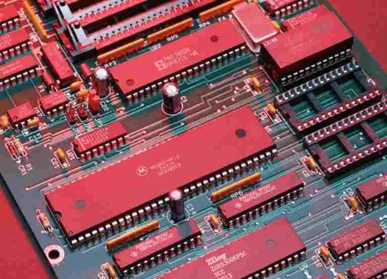
Necessity of PCB cleaning and smt parts processing
Every PCBA in a PCBA process must clean the equipment, because PCBA cleaning can greatly improve the efficiency and quality of the circuit board If PCBA is not cleaned, it will affect the reliability of the product
1. Appearance and power efficiency requirements
The most direct impact on PCBA pollution in PCBA processing plants is the appearance of PCBs If placed or used in a hot and humid environment, the residue may absorb moisture and turn white
Because lead-free chips, micro BGA, chip level packaging (CSP) and 01005 are widely used in components, the distance between components and circuit boards is reduced, the size is reduced, and the assembly density is increased. If halides are hidden under parts that cannot be cleaned, local cleaning may have disastrous consequences due to the release of halides.
Before PCBA surface coating, PCBA processes plants. Unclear resin residues will lead to delamination or cracking of the protective layer; The residue of active agent may cause electrochemical migration under the coating, which will lead to the failure of crack protection of the coating The research shows that cleaning can improve the adhesion rate of the coating by 50%
3. It needs to be cleaned if it is not cleaned
According to the current standard, the term "unclean" refers to that residues on the circuit board are safe from a chemical point of view, will not have any impact on the circuit board production line, and can be left on the circuit board. Corrosion, SIR, electromigration and other special detection methods are mainly used to determine the halogen/halide content, and then determine the safety of uncleaned parts after assembly.
However, even if the solid content of PCBA plant is low and there is no cleaning flux, there will still be more or less residues. For products with high reliability requirements, no residues or pollutants are allowed on the circuit board. For military applications, even electronic components need to be cleaned.
Advantages of SMD parts processing
SMT wafer processing has the advantages of high reliability and low solder joint defect rate. It can reduce external interference to the circuit board and is a very favorable link to achieve automation and increase output. At the same time, it can also save manpower and save a lot of resources for production.
Now, no matter what you do, you need efficiency. The patch processing can save human resources and improve efficiency. This technology will certainly be accepted by this industry, and science and technology are developing rapidly. No matter what industry, if it can not adapt to the environment well, it will be eliminated. Only when it is good enough, it will be left behind.
Electronic products are getting smaller and smaller, and we can't reduce the number of patches we used before. Now the function of this product will be more perfect. Traditional circuit can not meet these requirements. A large number of products can be produced by processing SMT wafers. The whole production is automatic, which can reduce costs, have good quality, meet market demand and improve market competitiveness.
SMT chip processing technology can meet the requirements of chip processing of various electronic components Many electrical appliances are made in this way, and the whole process is relatively simple Professional chip processing is mainly used for insulating materials of some large integrated circuits and transistors
Its density is relatively high and its mass is relatively small. Its total volume and weight account for about 0.1, which is traditionally common. Its volume is reduced by about half and its weight is reduced by about 60%. Its reliability is quite high, and it has a certain anti vibration ability. These characteristics can reduce electromagnetic and radiation interference, and greatly improve the utilization of raw materials.
And it can reduce energy consumption, reduce equipment use frequency, reduce manual working time, and greatly improve work efficiency. In this case, many coastal areas use this professional chip processing technology and vigorously develop electronic processing. After the technology is put into production, only a small amount of manpower can complete complex tasks, which is an important step in electronic production.
Testing and components after PCBA cleaning
Dec 28,2022


Just upload Gerber files, BOM files and design files, and the KINGFORD team will provide a complete quotation within 24h.