
Professional PCB manufacturing and assembly
Building 6, Zone 3, Yuekang Road,Bao'an District, Shenzhen, China
+86-13410863085Mon.-Sat.08:00-20:00

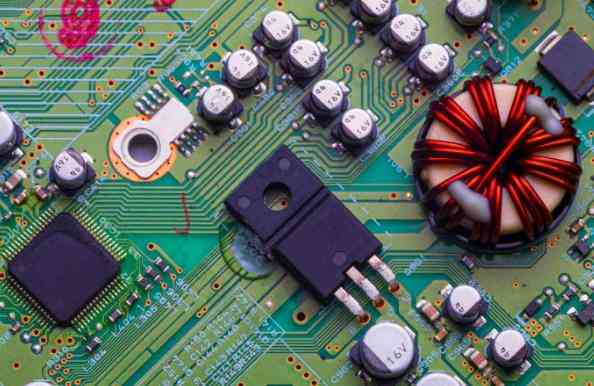
Basic requirements of SMT chip for component layout
1 Components shall be unified as far as possible in the printed SMT chip board Large mass components have a large heat capacity during reflow soldering Too high concentration is easy to cause local low temperature, leading to faulty welding; At the same time, the uniform layout is also conducive to the balance of the center of gravity In the vibration and impact test, components are not easy to be damaged, and holes and pads are metallized
2. Print the arrangement direction of components on the SMT terminal block. Similar components shall be arranged in the same direction as far as possible, and the characteristic direction shall be consistent, so as to facilitate the installation, welding and testing of components. For example, the anode of the electrolytic capacitor, the anode of the diode, the single pin end of the triode and the first pin of the integrated circuit are arranged in the same direction as far as possible. All part numbers are printed in the same direction.
3. The size of the heater head of the operable SMD repair equipment shall be kept around the large parts.
The heating elements should be located as far away from other components as possible and usually in corners and ventilated locations in the main housing.
5. Keep temperature sensitive parts away from heating parts. For example, 3-pole transistors, integrated circuits, electrolytic capacitors and some plastic housing components should be as far away from bridge stacks, high-power components, heat sinks and high-power resistors as possible.
6. The layout of parts and components that need to be adjusted or frequently replaced, such as potentiometers, adjustable inductance coils, variable capacitance microswitches, fuses, buttons, plugs and other components, should consider the overall structure, and should be placed in a position convenient for adjustment and replacement. If it is adjusted inside the machine, it should be placed on the printed circuit board that is easy to adjust; If the adjustment is made outside the machine, its position should be suitable for the position of the adjustment knob on the chassis panel to prevent conflicts between 3D space and 2D space. For example, the panel opening of the toggle switch and the vacant position of the switch on the printed circuit board should match.
7. Fixed holes shall be set at the center of terminals, inserts, long series terminals and near the parts that are often stressed. Corresponding space shall be reserved around the fixed holes to prevent deformation due to thermal expansion. If the thermal expansion of long series terminals is more serious than that of printed circuit boards, it is easy to warp during wave soldering.
8. Some parts (such as transformers, electrolytic capacitors, varistors, bridge stacks, radiators, etc.) and other parts that need secondary processing due to large volume (area) tolerance and low accuracy have a new range of intervals based on the original settings.
9. It is recommended to add a margin of not less than 1mm for electrolytic capacitors, varistors, bridges, polyester capacitors, etc., and a margin of not less than 3mm for transformers, radiators and resistors exceeding 5W (including 5W)
10. Electrolytic capacitors shall not contact heating elements, such as high-power resistance thermistors, transformers, radiators, etc. The minimum distance between electrolytic capacitor and radiator is 10mm, and the minimum distance between other elements and radiator is 20mm.
11. Do not place stress sensitive elements near corners, edges, or connectors, mounting holes, slots, notches, gaps, and corners of the printed circuit board. These locations are high stresses on the printed circuit board. In the area, it is easy to cause cracks or cracks in welding spots and components.
12. The layout of components shall meet the process requirements and spacing requirements of reflow and wave soldering. Reduce shadow effect during wave soldering.
13. The position of PCB positioning hole and fixing bracket shall be reserved.
14. When designing a large area printed circuit board with an area of more than 500cm2, in order to prevent the printed circuit board from bending in the tin furnace, a gap of 5-10mm wide should be left in the middle of the printed circuit board, and there should be no beads added to any component (can be wires) to prevent the printed circuit board from bending when passing through the tin furnace.
15. Element arrangement direction of reflow soldering process.
1. The placement direction of components shall consider the direction of PCB entering the reflux furnace.
2. In order to heat the welding end of the chip modules at both ends and the pins on both sides of the SMD module synchronously, the tombstone, displacement and welding end caused by simultaneous heating of the welding ends on both sides of the module are reduced. For welding defects such as magnets, the long axis of the chip assemblies at both ends of the printed circuit board shall be perpendicular to the conveyor belt direction of the reflux furnace.
3. The long axis of the SMD module shall be parallel to the conveying direction of the reflux furnace, and the long axis of the chip modules at both ends shall be perpendicular to the long axis of the SMD module.
4. In addition to the uniformity of heat capacity, good component layout design should also consider the arrangement direction and order of components.
5. For large size PCB, in order to make the temperature on both sides of PCB as consistent as possible, the long side of PCB should be parallel to the direction of reflux furnace conveyor belt. Recall that when the size of the printed circuit board is larger than 200mm, the requirements are as follows:
a) The long axis of the chip assemblies at both ends is perpendicular to the long edge of the printed circuit board.
b) The long axis of the SMD assembly is parallel to the long side of the printed circuit board.
c) The printed circuit boards assembled on both sides have the same direction of the components on both sides.
d) The arrangement direction of components on the printed circuit board. Similar components shall be arranged in the same direction as far as possible, and the characteristic direction shall be consistent, so as to facilitate the installation, welding and testing of components. For example, the anode of the electrolytic capacitor, the anode of the diode, the single pin end of the triode and the first pin of the integrated circuit are arranged in the same direction as far as possible.
16. The distance between the conductive patterns on the inner and outer edges of the PCB should be greater than 1.25 mm in order to prevent PCB processing due to interlayer short circuit caused by contacting the printed circuit during operation. When the outer edge of the PCB has been laid with ground wire, the ground wire can occupy the edge position For the position occupied by PCB due to structural requirements, no components and printed lines can be placed The bottom pad area of SMD shall be free of through-hole/SMC to avoid heating and remelting solder in wave soldering after reflow soldering diversion.
17. Installation spacing of components: the minimum installation spacing of components must meet the requirements for manufacturability, testability and maintainability of SMT patch components.


Just upload Gerber files, BOM files and design files, and the KINGFORD team will provide a complete quotation within 24h.