
Professional PCB manufacturing and assembly
Building 6, Zone 3, Yuekang Road,Bao'an District, Shenzhen, China
+86-13410863085Mon.-Sat.08:00-20:00

SMT solder paste printing problem, PCBA manufacturability
Solder paste printing is a complex process of SMT placement, and it is easy to have some shortcomings that affect the quality of the final product Therefore, in order to avoid some common faults in printing, we can avoid or solve the common shortcomings of SMT processing solder paste printing:
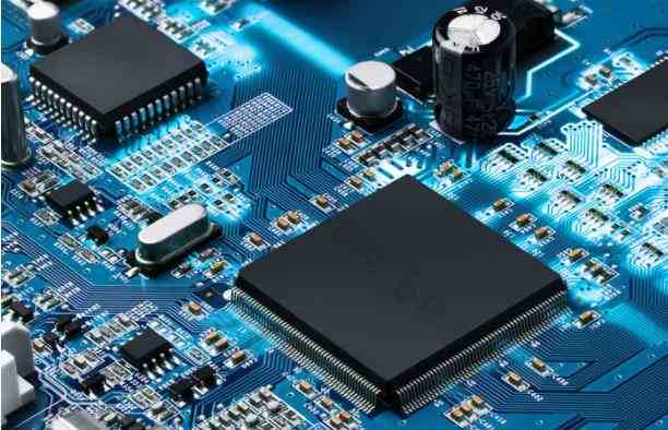
SMT patch
1. Draw the tip. Generally, the solder paste on the pad will be hilly after printing.
Cause: It may be caused by scraper clearance or solder paste viscosity.
Avoidance or solution: During SMT chip processing, the scraper gap should be appropriately reduced or the solder paste with proper viscosity should be selected.
2. Solder paste is too thin.
The reasons are as follows: 1. The model is too thin; 2. Excessive wiper pressure; 3. Poor liquidity of solder paste.
Avoidance or solution: select a template with appropriate thickness; Select the solder paste with appropriate fineness and viscosity; Reduce the pressure of the scraper.
3. After printing, the thickness of solder paste on the pad PCB pad changes
Avoidance or solution: fully mix solder paste before printing; Adjust the relative position of the template and the printed board.
Fourth, the thickness is different, and there are burrs on the edge and appearance.
Cause: It may be that the solder paste has low viscosity and the template hole wall is rough.
Avoidance or solution: choose a slightly higher viscosity solder paste; Check the etching quality of the template opening before printing.
5、 Autumn. After printing, the solder paste sinks to both ends of the pad.
Reason: 1. The scraper pressure is too high; 2. The printed board is not firmly positioned; 3. Solder paste viscosity or metal content is too low.
Avoidance or solution: adjust the pressure; Fix the printed board from the beginning; Select the solder paste with proper viscosity.
6. Incomplete printing means there is no solder paste printed on some parts of the pad.
The reasons are as follows: 1. The opening is blocked or part of the solder paste sticks to the bottom of the template; 2. Solder paste viscosity is too low; 3. There are large metal powder particles in the solder paste; 4. The scraper is worn.
Avoidance or solution: clean the opening and bottom of the template; Select the solder paste with proper viscosity, so that the solder paste printing can effectively cover the entire printing area; Select the solder paste with fine metal powder corresponding to the opening size; Check and replace the scraper.
Today I will introduce how to avoid or solve the common shortcomings of SMT paster printing. Operators understand the causes and solutions of these solder paste printing defects, and can avoid or quickly deal with these problems in work to ensure product quality.
In the daily SMT chip processing work, we usually handle PCBA processing. Understanding the concept of PCBA processing has become a necessary skill for high-quality SMT chip processing plants. In this article, we will introduce PCBA processing and manufacturability design to you, and we hope to help you.
1. Structure of PCBA
The structure of PCBA has a remarkable feature, that is, components are installed on one side or both sides of PCB. To facilitate communication, both sides of the PCBA are defined in IPC-SM-782. Generally, we call the side with more installation components and package types as the primary side (primary side); On the contrary, the mounting part surfaces with fewer package types are called secondary sides (secondary sides), which correspond to the top and bottom surfaces defined by the EDA layer sequence respectively.
Since the auxiliary assembly surface is usually welded first and then the main assembly surface, sometimes we also refer to the auxiliary assembly surface as the main welding surface and the main assembly surface as the secondary welding surface.
2. PCBA manufacturability design
The manufacturability design of PCBA mainly solves the assembly problem, aiming to achieve the shortest process path, the highest welding pass rate and the lowest production cost.
The design content mainly includes: process path design, assembly surface component layout design, pad and solder mask design (related to pass rate), assembly thermal design, assembly reliability design, etc. The process path is mainly determined according to the total number of parts used and packaging type, which determines the layout of components on the PCBA assembly surface.
3. PCB assembly
Print Circuit Board Assembly (PCB A) refers to a printed circuit assembly equipped with electronic components and having certain circuit functions It is also called a single board in an electronics factory
Solder paste printing is a complex process of SMT placement, and it is easy to have some shortcomings that affect the quality of the final product Therefore, in order to avoid some common faults in printing, we can avoid or solve the common shortcomings of SMT processing solder paste printing:
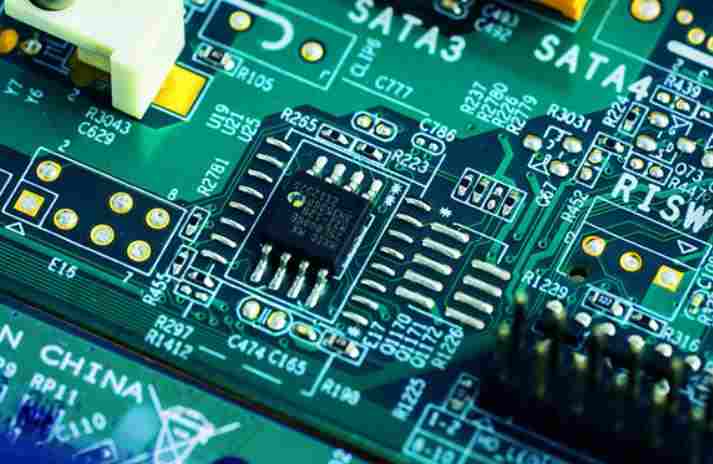
SMT patch
1. Draw the tip. Generally, the solder paste on the pad will be hilly after printing.
Cause: It may be caused by scraper clearance or solder paste viscosity.
Avoidance or solution: During SMT chip processing, the scraper gap should be appropriately reduced or the solder paste with proper viscosity should be selected.
2. Solder paste is too thin.
The reasons are as follows: 1. The model is too thin; 2. Excessive wiper pressure; 3. Poor liquidity of solder paste.
Avoidance or solution: select a template with appropriate thickness; Select the solder paste with appropriate fineness and viscosity; Reduce the pressure of the scraper.
3. After printing, the thickness of solder paste on the pad PCB pad changes

Avoidance or solution: fully mix solder paste before printing; Adjust the relative position of the template and the printed board.
Fourth, the thickness is different, and there are burrs on the edge and appearance.
Cause: It may be that the solder paste has low viscosity and the template hole wall is rough.
Avoidance or solution: choose a slightly higher viscosity solder paste; Check the etching quality of the template opening before printing.
5、 Autumn. After printing, the solder paste sinks to both ends of the pad.
Reason: 1. The scraper pressure is too high; 2. The printed board is not firmly positioned; 3. Solder paste viscosity or metal content is too low.
Avoidance or solution: adjust the pressure; Fix the printed board from the beginning; Select the solder paste with proper viscosity.
6. Incomplete printing means there is no solder paste printed on some parts of the pad.
The reasons are as follows: 1. The opening is blocked or part of the solder paste sticks to the bottom of the template; 2. Solder paste viscosity is too low; 3. There are large metal powder particles in the solder paste; 4. The scraper is worn.
Avoidance or solution: clean the opening and bottom of the template; Select the solder paste with proper viscosity, so that the solder paste printing can effectively cover the entire printing area; Select the solder paste with fine metal powder corresponding to the opening size; Check and replace the scraper.
Today I will introduce how to avoid or solve the common shortcomings of SMT paster printing. Operators understand the causes and solutions of these solder paste printing defects, and can avoid or quickly deal with these problems in work to ensure product quality.
In the daily SMT chip processing work, we usually handle PCBA processing. Understanding the concept of PCBA processing has become a necessary skill for high-quality SMT chip processing plants. In this article, we will introduce PCBA processing and manufacturability design to you, and we hope to help you.
1. Structure of PCBA
The structure of PCBA has a remarkable feature, that is, components are installed on one side or both sides of PCB. To facilitate communication, both sides of the PCBA are defined in IPC-SM-782. Generally, we call the side with more installation components and package types as the primary side (primary side); On the contrary, the mounting part surfaces with fewer package types are called secondary sides (secondary sides), which correspond to the top and bottom surfaces defined by the EDA layer sequence respectively.
Since the auxiliary assembly surface is usually welded first and then the main assembly surface, sometimes we also refer to the auxiliary assembly surface as the main welding surface and the main assembly surface as the secondary welding surface.
2. PCBA manufacturability design
The manufacturability design of PCBA mainly solves the assembly problem, aiming to achieve the shortest process path, the highest welding pass rate and the lowest production cost.
The design content mainly includes: process path design, assembly surface component layout design, pad and solder mask design (related to pass rate), assembly thermal design, assembly reliability design, etc. The process path is mainly determined according to the total number of parts used and packaging type, which determines the layout of components on the PCBA assembly surface.
3. PCB assembly
Print Circuit Board Assembly (PCB A) refers to a printed circuit assembly equipped with electronic components and having certain circuit functions It is also called a single board in an electronics factory
Operation procedure flow of mounting machine
Dec 28,2022


Just upload Gerber files, BOM files and design files, and the KINGFORD team will provide a complete quotation within 24h.