
Professional PCB manufacturing and assembly
Building 6, Zone 3, Yuekang Road,Bao'an District, Shenzhen, China
+86-13410863085Mon.-Sat.08:00-20:00

SMT processing quality and appearance inspection
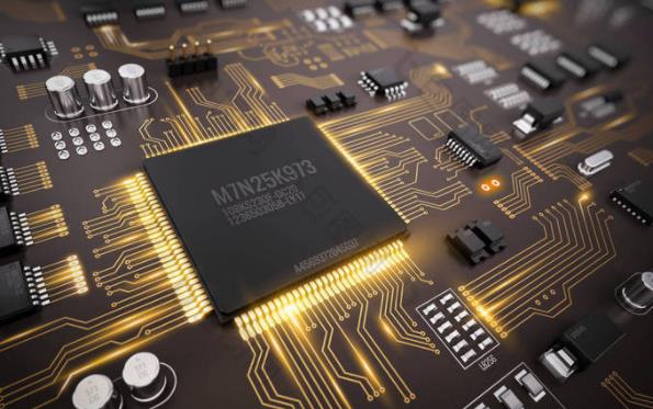
With the progress of science and technology, some electronic products, such as mobile phones and tablets, are moving towards lightweight Electronic components used for SMT processing are also becoming smaller Changed to give 0201. Dimension How to ensure the quality of solder joints has become an important issue in high-precision placement As a bridge for welding, the quality and reliability of solder joints determine the quality of electronic products In other words, in the production process, the quality of SMT is ultimately the quality of solder joints
At present, in the electronic industry, although the research of lead-free solder has made great progress, it has begun to be popularized and applied worldwide, and environmental protection issues have also been widely concerned. Soldering technology using tin lead solder alloy is still the main connection technology of electronic circuits.
(1) The surface is complete, smooth and glossy;
(2) An appropriate amount of solder and solder completely cover the welding part of the bonding pad and lead, and the component height is moderate;
(3) Good wettability; The edge of the solder joint shall be thin, and the wetting angle between the solder and the pad surface shall be less than 300, and the maximum shall not exceed 600.
SMT processing appearance inspection content:
(1) Whether the components are missing;
(2) Whether the parts are pasted incorrectly;
(3) Whether there is short circuit;
(4) Whether there is false welding; The causes of false welding are relatively complex.
1. Welding judgment
1. Use the special equipment of online tester for testing.
2. Visual inspection or AOI inspection. When there is too little solder in the solder joint, the solder penetration is poor, or there is a crack in the middle of the solder joint, or the solder surface protrudes, or the solder is incompatible with SMD. The presence of a large number of false welds should be judged immediately. The judgment method is: check whether there are many problems with solder joints at the same position on the PCB. If this is only a problem on a single PCB, it may be caused by solder paste scratching, pin deformation, etc., such as the same position on many PCBs. There are some problems. At this time, it is likely to be caused by poor components or gasket problems.
3. Causes of faulty soldering and solutions
1. Defective gasket design The through hole on the pad is a major defect in PCB design during welding Do not use them if they are not absolutely necessary Through hole will lead to solder loss and solder shortage; The pad spacing and area also need standard matching, otherwise, the design should be corrected as soon as possible
2. PCB board is oxidized, that is, the bonding pad is black and does not emit light. If oxidation is present, an eraser can be used to remove the oxide layer to reproduce bright light. If the PCB board is wet, it can be dried in the drying box if it is suspected to be wet. PCB board is polluted by oil stain, sweat stain, etc. At this time, wash with absolute ethanol.
SMT development trend and leading components
Dec 06,2022


Just upload Gerber files, BOM files and design files, and the KINGFORD team will provide a complete quotation within 24h.