
Professional PCB manufacturing and assembly
Building 6, Zone 3, Yuekang Road,Bao'an District, Shenzhen, China
+86-13410863085Mon.-Sat.08:00-20:00

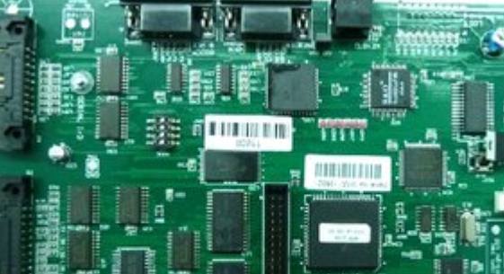
Causes and Solutions of SMT Short Circuit
The reason and solution of short circuit in SMT wafer processing SMT short circuit mainly occurs between pins of small pitch integrated circuits, so it is also called "bridge" Of course, there is also a short circuit between chip components, which is very rare Now, let's talk about the causes and solutions of bridging problems between pins of small pitch integrated circuits The bridging phenomenon mainly occurs between IC pins with a spacing of 0. 5mm or less Because the court is very small, it is easy to have minor omissions when the model is improperly designed or printed A This model is based on the requirements of IPC-752.5 Steel Fabric Design Guide To ensure that the solder paste can be released smoothly from the template opening to the PCB pad, the mold opening mainly depends on three factors:
1.) Area ratio/width thickness ratio>0.66 2.) The grid wall is smooth.
The supplier needs to conduct electrolytic polishing during production 3.) With the printing surface as the upper side, the lower opening of the grid should be 0.01 mm or 0. 02 mm wider than the upper opening, that is, the opening is inversely tapered to facilitate the effective release of solder paste and reduce the frequency of cleaning the screen Specifically, for IC with spacing of 0 5 mm and below, because their pitch is very small, it is easy to bridge. The length of the mold opening method remains unchanged, and the opening width is 0.5 to 0.75 pad width The thickness is 0.12~0.15 mm It is better to use laser cutting and polishing to ensure that the opening shape is inverted trapezoid and the inner wall is smooth, so that the color and shape are good during printing B. The correct selection of solder paste is also very important to solve the bridging problem When using an integrated circuit solder paste with a pitch of 0 5mm and below, the fineness shall be 20~45um, and the viscosity shall be about 800~1200pa. The activity of solder paste can be determined according to the cleanliness of solder, and RMA grade is usually used C. Printing is also a very important part
(1) Scraper type: There are two kinds of scraper: plastic scraper and steel scraper. For integrated circuits with a spacing of – 0 5mm, steel scraper shall be used for printing to facilitate the formation of solder paste after printing (2) Adjustment of the wiper plate: the working angle of the wiper plate is printed in the 45 ° direction, which can significantly improve the imbalance of different mold opening directions of the solder paste, and can also reduce the damage to the opening of the fine spacing template; The pressure of the scraper is usually 30N/mm ². (3) Printing speed: Solder paste rolls forward on the template with the help of the scraper. Fast printing speed is conducive to the rebound of the template, but at the same time, it will block the solder paste from being printed If the speed is too slow, the solder paste will not roll on the template, resulting in low resolution of solder paste printed on the pad The printing speed range of asphalt is 10-20 mm/s (4) printing pipeline: at present, the most common printing methods are "contact printing" and "non-contact printing" The printing method with gap between the template and PCB is "non-contact printing" Generally, the clearance value is 0.5~1.0mm, which has the advantage of being suitable for solder pastes with different viscosities The solder paste is pushed into the template opening by the scraper and contacts with the PCB pad After slowly removing the scraper, the template will automatically separate from the PCB, which can reduce the template pollution problem caused by vacuum leakage The printing method without gap between the template and PCB is called "contact printing" It requires the stability of the overall structure and is suitable for printing high-precision solder paste The template keeps very flat contact with the PCB, only with the printed PCB Therefore, the printing accuracy achieved by this method is high, and it is particularly suitable for fine pitch, Ultra fine pitch solder paste printing D. Installation height For integrated circuits with a spacing of – 0 5mm, 0 distance or 0-0. The installation height of 1mm should be used during installation to avoid the collapse of solder paste forming due to the low installation height Short circuit during return E. Reflow 1. The heating speed is too fast 2. The heating temperature is too high 3. The heating speed of solder paste is faster than that of circuit board 4. The wetting speed of flux is too fast
The above is the explanation given by the editor of pcb circuit board company.
If you want to know more about PCBA, you can go to our company's home page to learn about it.
In addition, our company also sells various circuit boards,
High frequency circuit board and SMT chip are waiting for your presence again.


Just upload Gerber files, BOM files and design files, and the KINGFORD team will provide a complete quotation within 24h.