
Professional PCB manufacturing and assembly
Building 6, Zone 3, Yuekang Road,Bao'an District, Shenzhen, China
+86-13410863085Mon.-Sat.08:00-20:00

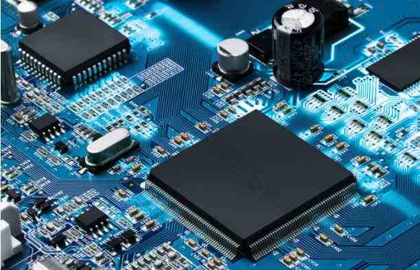
Surface mount technology and surface mount technology
Surface mounting process
SMT basic process components include: screen printing (or distribution), placement (curing), reflow, cleaning, testing and maintenance
1. Silk screen printing: Its function is to leak solder paste or repair glue onto PCB pad to prepare for component welding. The equipment used is the screen printing machine (screen printing machine) located at the front end of the SMT production line.
2 Glue dispensing: drop glue on the fixed position of PCB board, whose main function is to fix components on PCB board The equipment used is glue distributor, which is located behind the SMT production line or test equipment
3. Installation: Its function is to accurately install surface mounted components to the fixed position of PCB. The equipment used is the mounting machine, which is located behind the screen printing machine in the SMT production line.
4. Curing: Its function is to melt the patch adhesive, so that the surface assembly components and PCB board are firmly bonded together. The equipment used is a curing furnace, which is located behind the SMT mounter in the SMT production line.
Polychlorinated biphenyls
5. Reflow soldering: Its function is to melt the solder paste, so that the surface mounted components and PCB board are firmly bonded together. The equipment used is a reflux furnace, which is located behind the SMT mounter in the SMT production line.
6. Cleaning: Its function is to remove solder residues harmful to human health on the assembled PCB, such as flux. The equipment used is a washing machine, which may not be fixed in position. It may be opening or closing the line
7. Check: Its function is to check the welding quality and assembly quality of the assembled PCB. The equipment used includes magnifying glass, microscope, on-line tester (ICT), flying probe tester, automatic optical inspection (AOI), X-ray testing system, function tester, etc. It can be configured at the appropriate position on the production line according to the detection needs.
8. Rework: Its function is to rework PCB boards without detected faults. The tools used are soldering irons, rework stations, etc. that are equipped anywhere on the production line.
SMT mounting process
Single side assembly
Incoming inspection=>screen solder paste (spot adhesive)=>patch=>drying (curing)=>reflow soldering=>cleaning=>inspection=>repair
Double sided assembly
A: Incoming inspection=>PCB A-side screen solder paste (spot SMD glue)=>SMD PCB B-side screen solder paste (spot SMD glue)=>SMD=>drying=>reflow soldering (preferably only applicable to B-side=>cleaning=>inspection=>repair).
B: Incoming inspection=>PCB side A screen solder paste (spot patch adhesive)=>SMD=>drying (curing)=>A-side reflow soldering=>cleaning=>turnover rate=PCB side B spot patch adhesive=>patch=>curing=>B surface wave soldering=>cleaning=>inspection=>repair)
This process is applicable to reflow soldering on the A side of PCB and wave soldering on the B side. In SMDs assembled on the B side of PCB, this process should be used when there are only SOT or SOIC (28) pins or fewer.
3. Single side mixed packaging process:
Incoming inspection=>PCB A-side screen solder paste (patch adhesive)=>SMD=>drying (curing)=>reflow soldering=>cleaning=>parts=>wave soldering=>cleaning=>inspection=>rework
4. Double sided mixed packaging process:
A: Incoming inspection=>PCB's B side point stain glue=>SMD=>curing=>flip board=>PCB's A side plug-in=>wave solving=>cleaning=>inspection=>rework
Paste before inserting, applicable to the case where SMD components are more than individual components
B: Incoming inspection=>PCB side A parts (pin bending)=>Flip board=>PCB side B paster=>paster=>curing=>Flip board=>wave soldering=>cleaning=>inspection=>repair
First insert, then paste, applicable to the case where there are more independent components than SMD components
C: Incoming inspection=>PCB A-side screen solder paste=>patch=>drying=>reflow soldering=>parts, pin bending=>turnover=>PCB B-point patch adhesive=>patch=>curing=>flipping=>wave soldering=>cleaning=>inspection=>rework A-side hybrid assembly, B-side installation.
D: Incoming inspection=>PCB B side point paster=>SMD=>curing=>turnover=>PCB A side wire mesh solder paste=>paster=>A side reflow=>parts=>B side wave soldering=>cleaning=>inspection=>rework A side and B side mixed installation. First, paste on both sides of the SMD, reflow, and then insert it. Wave soldering E: incoming inspection=>PCB B-side wire mesh solder paste (spot paste)=>SMD=>drying (curing)=>reflow soldering=>flip board=>PCB A-side wire mesh solder paste=>SMD=>drying=reflow soldering 1 (partial welding can be used)=>parts=>wave soldering 2 (manual welding can be used if there are few components)=>cleaning=>inspection=>rework A-side installation and B-side mixed installation.
5、 Double side assembly process
A: Incoming material inspection, PCB A-side screen solder paste (spot adhesive), patch, drying (curing), A-side reflow, cleaning, and flipping; PCB B side screen solder paste (spot patch adhesive), patch, drying, reflow (preferably only used for B side, cleaning, testing, maintenance)
When a large patch such as PLCC is connected to two patches, this process is applicable to picking up the side of a PCB
B: Incoming inspection, PCB A-side screen solder paste (dot stain adhesive), repair, drying (curing), A-side reflow, cleaning, turning; PCB B side spot patch adhesive, patch, curing, B-side wave soldering, cleaning, inspection, rework) This process is applicable to the reflow soldering of PCB A side.
Rework of common patch in patch processing
Dec 06,2022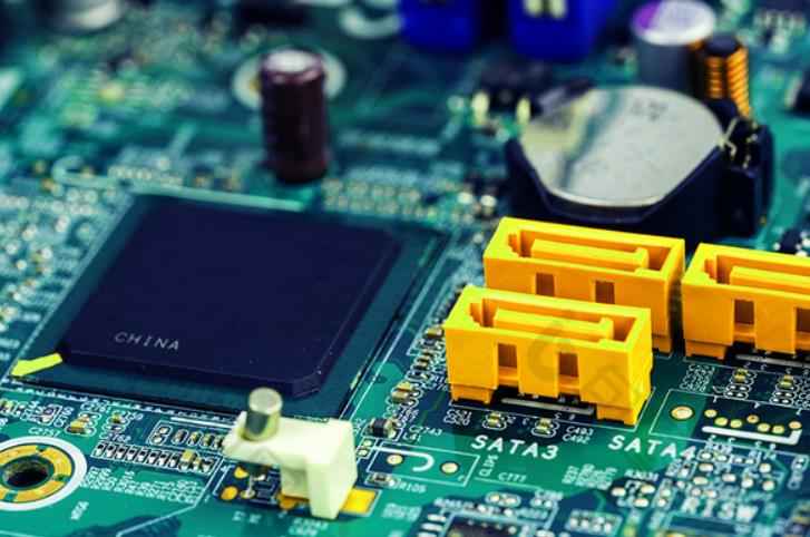


Just upload Gerber files, BOM files and design files, and the KINGFORD team will provide a complete quotation within 24h.