
Professional PCB manufacturing and assembly
Building 6, Zone 3, Yuekang Road,Bao'an District, Shenzhen, China
+86-13410863085Mon.-Sat.08:00-20:00

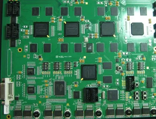
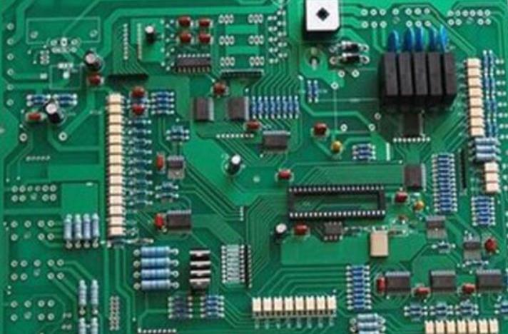
Follow the PCB layout principle of "big first, small second, difficult first, easy second", that is, important unit circuits and core components should be arranged first 2. The layout shall refer to the principle block diagram and arrange the main components according to the main signal flow direction of the board 3. The arrangement of PCB components shall be easy to adjust
Follow the layout principle of "large before small, difficult before easy", that is, important unit circuits and core components should be arranged first
2. The PCB layout shall refer to the schematic block diagram and arrange the main components according to the main signal flow direction of the board
3. PCB components shall be arranged to facilitate debugging and maintenance, that is, large components shall not be placed around small components, and enough space shall be provided around components to be debugged.
4. For circuits with the same structure, "symmetrical" standard layout shall be adopted as far as possible;
5. Optimize the layout according to the standard of uniform distribution, balance of gravity center and beautiful layout;
6. Plug in components of the same type shall be placed in one direction in the X or Y direction. Polarized discrete components of the same type shall also strive to be consistent in the X or Y direction, so as to facilitate production and inspection.
7. The heating elements should generally be evenly distributed to facilitate the heat dissipation of the single board and the whole machine. The temperature sensitive devices other than the temperature detection components should be far away from the components with large heat.
8. The layout shall meet the following requirements as far as possible: the total wiring shall be as short as possible, and the key signal lines shall be as short as possible; High voltage, high current signal and low current, low voltage weak signal are completely separated; Separate analog signal from digital signal; High frequency signal is separated from low frequency signal; The spacing of high-frequency PCB components shall be sufficient.
9. The PCB layout of the decoupling capacitor should be as close to the power supply pin of the IC as possible, and the circuit formed between it and the power supply and ground should be the shortest.
10. When arranging PCB components, it should be properly considered that the components using the same PCB power supply should be placed together as much as possible to facilitate the separation of power supply in the future.


Just upload Gerber files, BOM files and design files, and the KINGFORD team will provide a complete quotation within 24h.