
Professional PCB manufacturing and assembly
Building 6, Zone 3, Yuekang Road,Bao'an District, Shenzhen, China
+86-13410863085Mon.-Sat.08:00-20:00

Advantages and disadvantages of Smt test (ICT) and SPI
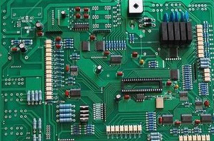
In smt chip processing, it is not only to place components on designated PCB pads If you want to get good quality and customer representation, obviously, this is not enough We must obtain sufficient data through various test methods to obtain specific test data and records to support our quality requirements At this time, various detection technologies and methods become very important
From the perspective of smt processing plant, this paper discusses the related issues of online testing (ICT). On line testing (ICT) is usually used to detect the direction of a circuit board, such as open circuit, resistance, capacitance and components, but it is also a relatively less used device. What are the specific advantages and disadvantages?
ICT test
As we all know, online testing or ICT works by using a set of probes to access circuit nodes and then checking the performance of each component. It can also test the function of digital circuits, but the cost involved is very high.

Generally, ICT has the advantage of testing a large number of products It can also be used to test well developed products However, because ICT needs to create custom devices, the cost and lead time involved are high However, the advantage of ICT is that once you prepare the customized tools, the organizational cost will be very low, but the cost of small batch PCB processing is obviously very high
If we summarize the advantages and disadvantages of ICT, they will be as follows:
Advantages:
1. It is helpful to quickly test each PCBA device
2. Low organizational costs.
3. You can test individual components.
4. It works well when you need to test logical functionality.
5. Can be used to test LED components.
6. You can use it to test the welding of BTC components by stress testing.
Disadvantages:
1. The lead time required for development is usually very long, which may be a problem in today's era when fast time to market becomes a source of competitive advantage.
2. The high upfront cost may be unfavorable to its use
3. Programming tools are required.
4. You cannot use it to test non electric components or connectors
5. Although it can be used to test individual components, it is not suitable for testing components that work together.
Advantages of SPI in Smt Processing
The pursuit of high reliability and efficiency of SMT processing (surface mount technology) assembly has always been the goal of electronic manufacturers' expectation consistency. This depends on the optimization of every detail in the whole process. As far as SMT assembly is concerned, it can be concluded that 64% of the defects are caused by incorrect solder paste printing. In addition, defects lead to low product reliability and reduce its efficiency. Therefore, it is necessary to conduct high-performance solder paste printing to minimize the possibility of low quality.
Inspection is a necessary measure to meet the SMT assembly requirements. At present, common inspection methods include visual inspection, AOI (Automatic Optical Inspection), X-ray inspection, etc. In order to prevent improper solder paste printing from reducing the efficiency of the final product, solder paste inspection (SPI) solder paste printing during SMT assembly should be carried out after welding.
Based on 20 years of electronic manufacturing experience, Jingbang has won a good reputation in the world electronics industry for its deep concern for product reliability. Jingbang Electronic's one-stop PCB processing includes PCB manufacturing, component procurement and smt chip assembly. Smooth operation comes from strict process control in the workshop.
SPI usually appears after the solder paste is printed, so that printing defects can be found in time to correct or eliminate defects before placement. Or, it may lead to more defects or even disasters in the later period.
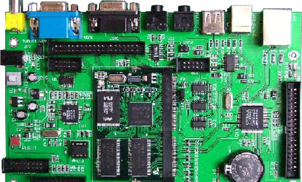
PCBA processing
Advantages of SPI
1. Reduce defects
SPI is used for the first time to reduce defects caused by improper solder paste printing. Recall that SPI's main advantage lies in its ability to reduce defects. As far as SMT assembly is concerned, defects have always been a major problem. The reduction of its quantity will lay a solid foundation for high reliability of products.
2. High efficiency
Consider the traditional SMT assembly process rework model Unless inspection is carried out, that is, it will not expose any defects Usually, AOI or X-ray inspection is used to find defects and then rework If SPI is used, defects can be found at the beginning of SMT assembly process after printing solder paste Once the solder paste is found to be printed incorrectly, it can be reworked immediately to obtain high-quality PCB solder paste printing It will save more time and improve manufacturing efficiency
3. Low cost
For the application of SPI machine, low cost has two meanings. On the one hand, since defects can be found at the early stage of the SMT assembly process and rework can be completed in time, the time cost will be reduced. On the other hand, since the defects can be stopped in advance to avoid delaying the early defects to the later manufacturing stage, resulting in threatening defects, this will also reduce capital.
Fourth, high reliability
Most defects in SMT assembly products originate from low quality PCB solder paste printing. Since SPI helps to reduce defects, it will help improve the reliability of PCB products by strictly controlling defect sources.


Just upload Gerber files, BOM files and design files, and the KINGFORD team will provide a complete quotation within 24h.