
Professional PCB manufacturing and assembly
Building 6, Zone 3, Yuekang Road,Bao'an District, Shenzhen, China
+86-13410863085Mon.-Sat.08:00-20:00

The importance of smt printing and x-ray in smt processing
According to statistics, more than 60% of defective repair welding is caused by defective solder paste printing, so solder paste printing is very important The quality of solder paste printing determines the efficiency of the whole production line and the passing rate of high-quality products. In order to improve the efficiency of the whole production line and reduce welding defects, engineers SMT processing plants need to analyze and improve printing defects to reduce welding defects caused by poor printing
Common Defects and Improvement Measures of SMT Solder Paste Printing
1. Solder paste collapse
The solder paste cannot maintain a stable shape, the edge collapses and flows to the outside of the pad, and is connected between adjacent pads. This phenomenon may cause solder short circuit.
Reasons and improvement measures
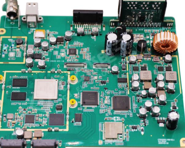
Circuit board

1. If the scraper pressure is too high, the solder paste will be squeezed and flow into the adjacent pad after passing through the steel mesh hole. Improvement measures: reduce scraper pressure
2. The viscosity of solder paste is too low to maintain the fixed printing shape of solder paste. Improvement measures: use solder paste with high viscosity
3. The tin powder is too small, the tin powder is too small, and the solder paste has good efficiency, but the solder paste molding is insufficient. Improvement measures: choose the solder paste with larger tin powder particles
Second, solder paste offset
Solder paste misplacement means that the printed solder paste is not fully aligned with the specified pad position, which may lead to bridging, or may cause the solder paste to be printed on the solder mask, thus forming solder balls
Reasons and improvement measures
1. PCB board is supported or not clamped, which may lead to die alignment and holes when PCB pad is printing solder paste scraper, and solder paste printing seems to be offset printing Improvement measures: use multi-point clamping to fix the PCB board
2. There is deviation between PCB incoming material and mold opening. The quality of the mold opening may be poor and deviated from the designated position of the PCB pad. Improvement: Reopen the grid accurately
Third, solder paste missing
Solder paste leakage means that the solder paste coverage area of the pad is less than 80% of the opening area, resulting in insufficient solder on the pad or no printed solder paste on the pad
Reasons and improvement measures
1. The scraper speed is too fast, which leads to insufficient filling of solder paste vias, especially PCB and steel mesh with small pads and holes. Improvement measures: reduce the speed of scraper
2. The separation speed is too fast. After the solder paste is printed, the separation speed is too fast, causing the solder paste on the bonding pad to be removed, resulting in missing printing or sharpening.
Improvement measures: adjust the separation speed to a reasonable range
3. The solder paste viscosity is too high, and the solder paste printing is not enough to flow into the pad position of the corresponding hole. Improvement measures:
Select solder paste with proper viscosity
4. The opening of the template is too small, the opening of the template is small, and the scraper speed is fast, resulting in insufficient tin removal and solder paste leakage. Improvement measures: precision wire mesh tapping
Importance of X-ray in smt processing industry
X-ray, full name is X-ray nondestructive testing equipment. Similar to the chest X-ray machine in the hospital, it mainly uses X-ray scanning and imaging inside the product, especially for detecting BGA QFN and other components with pins to detect whether there are cracks, foreign matters, virtual welding, false welding and other defects.
With the development of electronic technology, PCBA is everywhere. Every electronic product must have a fast PCBA. In retrospect, the application of chip technology is becoming more and more extensive. Intelligence and miniaturization make the size of chips smaller and smaller There are more and more pins Especially some core BGA and IC components are widely used
Ordinary manual inspection cannot fundamentally determine the quality of solder joints. AOI test equipment can only detect the welding components on the PCBA surface, but cannot detect the welding quality inside the pins passing through the circuit board. High precision electronic products require very high reliability. High, such as military, aviation, automotive electronics, then the best choice is through X-ray inspection.
In terms of application, X-ray can not only identify welding defects inside BGA (such as empty welding and virtual welding), but also scan and analyze microelectronic systems and sealing components, cables, clamps and plastic interior.

Methods and measures to reduce chip loss
Dec 02,2022


Just upload Gerber files, BOM files and design files, and the KINGFORD team will provide a complete quotation within 24h.