
Professional PCB manufacturing and assembly
Building 6, Zone 3, Yuekang Road,Bao'an District, Shenzhen, China
+86-13410863085Mon.-Sat.08:00-20:00


SMT patch reflow replacement process
SMT Chip Manufacturer Discussion on Factors Affecting SMT Chip Reflow Soldering Quality
Reflow soldering is one of the key processes in SMT processing. The result of reflow soldering directly reflects the quality of surface assembly. It is necessary to understand the factors that affect the quality of reflow soldering.
The welding quality problem in reflow soldering is not entirely caused by reflow soldering process, because the quality of reflow soldering is not only directly related to the welding temperature (temperature distribution), but also closely related to the equipment conditions of the production line, PCB pad and productivity design, solderability of components, quality of solder paste, quality of PCB processing, and process parameters of each SMT process, and even the operator's operation.
SMT chip assembly quality and PCB pad design If the PCB pad design is correct, a small amount of tilt during installation can be corrected due to the surface tension of molten solder during reflow soldering (called self positioning or self correcting effect) On the contrary, if the PCB pad design is incorrect, even if the installation position is very accurate, there will be component position deviation, suspension bridge and other welding defects after reflow soldering
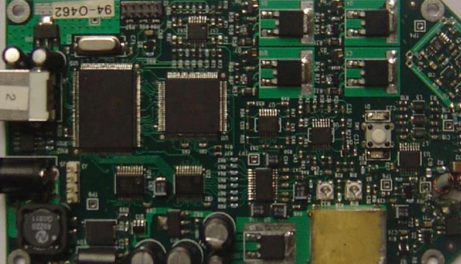
pcb board

1. Key elements of PCB pad design:
According to the structural analysis of solder joints of each component, in order to meet the reliability requirements of solder joints, PCB pad design should master the following key elements:
(1) The pads at both ends of the symmetry must be symmetrical to ensure that the surface tension of the molten solder is balanced.
(2) The pad spacing ensures the overlapping size between the component end or the lead and the pad. Too large or too small pad spacing will lead to welding defects.
(3) The remaining size of the pad must overlap the remaining size of the end of the part or the lead after the pad. The remaining size must ensure that the solder joint can form a meniscus.
(4) The width of the pad shall be approximately the same as the width of the component end or lead.
2. Defects easy to reflow:
If the design requirements are violated, welding defects will occur during reflow soldering, and PCB pad design problems are difficult or even impossible to solve in the production process. Take rectangular chip assembly as an example:
(1) When the gap between pads G is too large or too small, because the welding end of the assembly cannot overlap with the pad during reflow welding, suspension bridges and displacements will occur.
(2) When the dimensions of the lining are asymmetric, or the ends of two parts are designed on the same lining, suspension bridges and displacements may also occur due to asymmetric surface tension.
(3) The pad is designed with a through hole, and the solder will flow out of the through hole, resulting in insufficient solder paste.
Data replacement process in SMT chip production
During the processing of SMT chips, due to the small order volume and frequent line changes, feeding and refueling are inevitable. In this process, there must be a strict standardization process to avoid incorrect data updates on the high-frequency replacement line during the data replacement process. What is the standard process to avoid replacing incorrect data? Let's analyze with you today:
1. Remove the tray and remove the used tray.
2. SMT operators can take materials from the material rack according to their own positions.
3. The operator uses the job number and location table to check the removed data to confirm whether the specification and model are the same.
4. The operator checks the new pallet and the old pallet to see if the specifications and models of the two pallets are identical.
5. The operator checks his data to indicate whether the company is consistent with the pallet.
6. If there is any abnormality in the above inspection, the mounter operator shall immediately notify the delay processing.
7. Take samples from the new pallet, and then place the data on the new pallet and the old pallet.
8. Paste the newly installed Feida data on the "refueling process record form", and fill in the refueling time, operator management and other relevant data and information.
9. Put the feeder back to the SMT mounter according to the SMT mounter station; You must fill in your supplementary information effectively and record it once.
10. The operator shall inform the project quality control personnel of data matching and testing, and must change and check the data.
11. IPQC checks whether the data and information are correct and whether the website is correct according to the website number list.
12. Before starting production, the operation inspection of the above mounter has been completed.
The above 12 steps are the SMT refueling process of the whole process, and the patch handling must be strictly followed Each step of the process must describe each post Only in this way can we avoid replacing the wrong data


Just upload Gerber files, BOM files and design files, and the KINGFORD team will provide a complete quotation within 24h.