
Professional PCB manufacturing and assembly
Building 6, Zone 3, Yuekang Road,Bao'an District, Shenzhen, China
+86-13410863085Mon.-Sat.08:00-20:00

The Development Trend of SMT Technology and the Disadvantages of Avoiding Solder Paste
Trend chip mounter
After more than 20 years of development, surface mount technology has become the component level interconnection of modern electronic engineering for PCB circuits Relevant data show that the popularity of SMT application in developed countries has exceeded 75%, and it has further developed into an assembly technology field represented by high-density assembly and 3D assembly The continuous development of assembly technology will inevitably put forward new requirements for the development of assembly technology and related equipment How to shorten the running time, speed up the conversion time, and constantly introduce components with a large number of pins and fine pitch has become a serious challenge for placement equipment today It is a very difficult decision to choose a suitable placement device to meet the needs of today's applications, but this is a very important choice, because the production capacity and multi-function adaptability of electronic works depend on the placement device Quite large
In order to improve the production efficiency and reduce the working time, the new mounter is developing towards the direction of efficient two-way conveying structure.
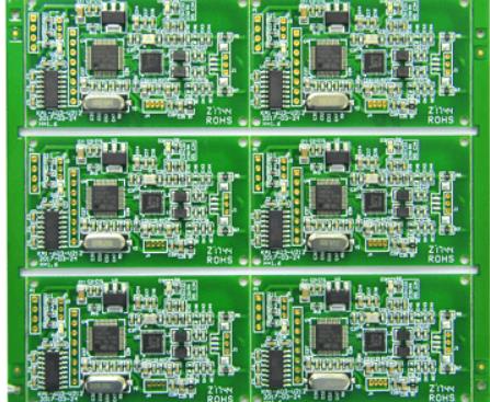
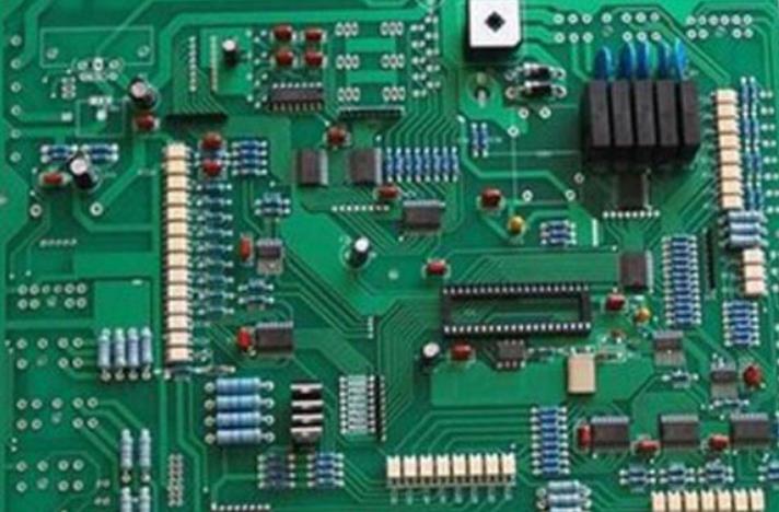
Circuit board

On the basis of maintaining the efficiency of traditional single path placement machine, dual channel conveyor placement machine is designed for PCB transportation, positioning, detection, placement, etc Enter the dual path structure
In order to improve the adaptability and efficiency, the new placement machine is developing towards flexible placement system and modular structure. The placement machine is divided into control host and functional module machine. The module machine has different functions. According to the placement requirements of different parts, they can be placed according to different precision and efficiency to achieve higher efficiency; When users have new requirements, they can add new functional modules as required. Because it can flexibly add different types of placement units according to future needs to meet future flexible production needs, this modular structure machine is very popular with customers. During work adjustment, it is very important to improve the working adaptability of the equipment in time. Importantly, new packaging and circuit boards bring new requirements. Investment in implanted equipment should generally be based on current considerations and estimates of future needs. Buying equipment with capabilities far beyond current requirements can often avoid missed opportunities in the future. Upgrading existing equipment is more cost-effective than buying new equipment.
Avoid the disadvantage of solder paste printing during SMT processing
Solder paste printing is a complex process in SMT chip processing, which is prone to some shortcomings and affects the quality of the final product. In order to avoid some common faults in printing, common disadvantages of SMT processing solder paste printing can be avoided or solved:
1. Draw the tip. Generally, the solder paste on the pad will be hilly after printing.
Cause: It may be caused by scraper clearance or solder paste viscosity.
Avoidance or solution: During SMT chip processing, properly adjust the scraper clearance or select the solder paste with proper viscosity.
2. Solder paste is too thin.
The reasons are as follows: 1. The model is too thin; 2. Excessive wiper pressure; 3. Solder paste has poor fluidity.
Avoidance or solution: select a template with appropriate thickness; Select the solder paste with appropriate fineness and viscosity; Reduce the pressure of the scraper.
3. After printing, the solder paste thickness on the PCB pad will change.
Reason: 1. The solder paste is mixed unevenly, and this particle size is uncommon. 2. The template is not parallel to the printed board;
Avoidance or solution: fully mix solder paste before printing; Adjust the relative position of the template and the printed board.
Fourth, the thickness is different, and there are burrs on the edge and appearance.
Cause: It may be that the solder paste has low viscosity and the template hole wall is rough.
Avoidance or solution: choose a slightly higher viscosity solder paste; Check the etching quality of the template opening before printing.
5、 Autumn. After printing, the solder paste sinks to both ends of the pad.
Reason: 1. Excessive scraper pressure; 2. The printed board is not firmly positioned; 3. Solder paste viscosity or metal content is too low.
Avoidance or solution: adjust the pressure; Fix the printed board from the beginning; Select the solder paste with proper viscosity.
6. Incomplete printing means that the solder paste is not printed on the PCB pad
The reasons are as follows: 1. The hole is blocked or part of the solder paste sticks to the bottom of the template; 2. Solder paste viscosity is too low; 3. There are large metal powder particles in the solder paste; 4. The scraper is worn.
Avoidance or solution: clean the opening and bottom of the template; Select the solder paste with proper viscosity, so that the solder paste printing can effectively cover the entire printing area; Select the solder paste with fine metal powder corresponding to the opening size; Check and replace the scraper.


Just upload Gerber files, BOM files and design files, and the KINGFORD team will provide a complete quotation within 24h.