
Professional PCB manufacturing and assembly
Building 6, Zone 3, Yuekang Road,Bao'an District, Shenzhen, China
+86-13410863085Mon.-Sat.08:00-20:00

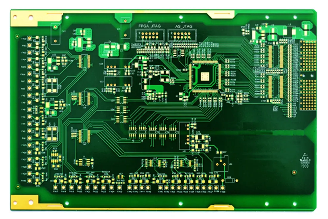
Analysis of Electrical Reliability in PCBA
The electrical and PCB circuit boards in PCBA are generally processed by SMT, followed by flow soldering, wave soldering, rework and other processes.
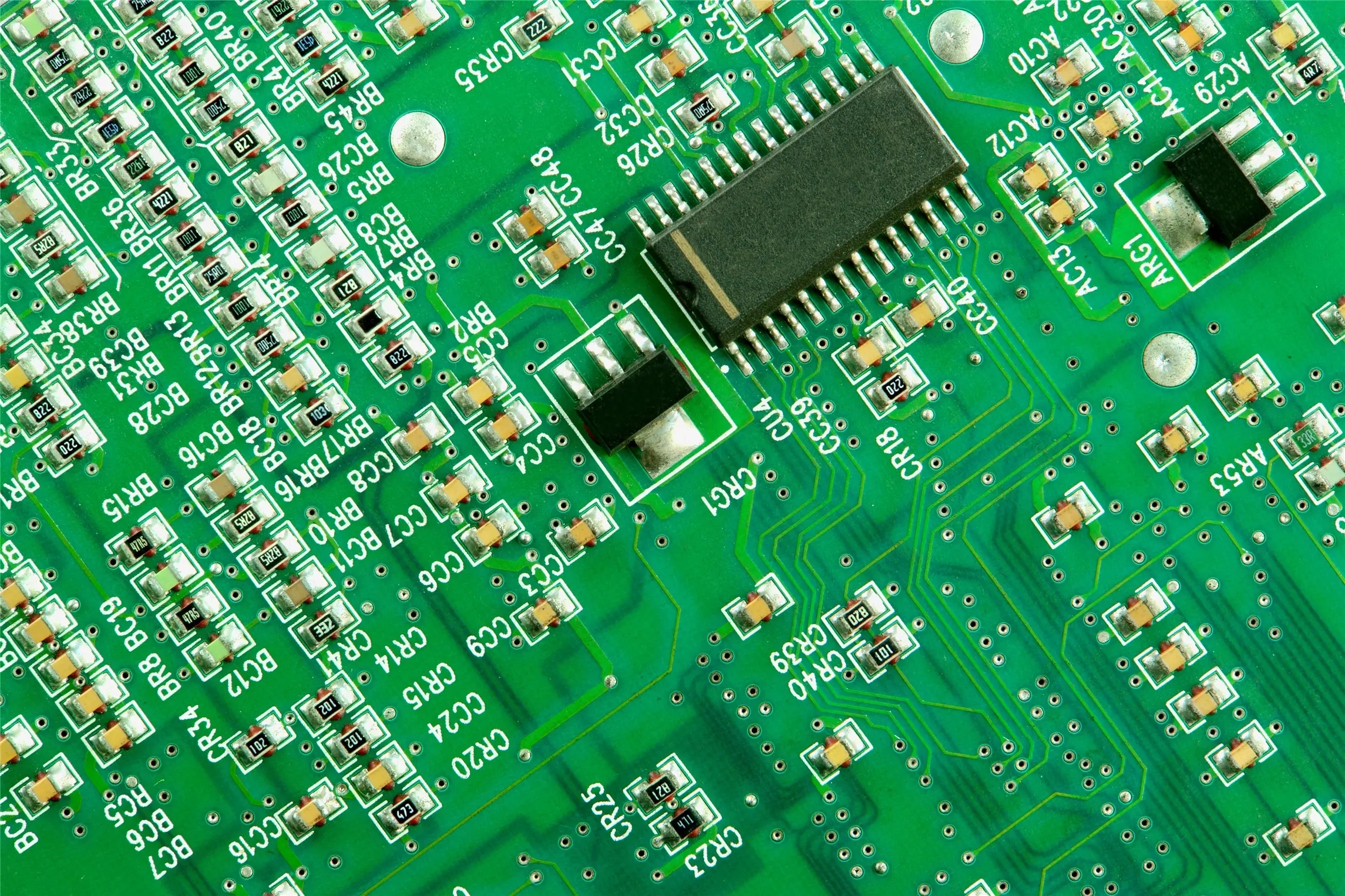
The same PCB is generally processed by SMT, and then through flow soldering, wave soldering, rework and other processes. It is likely to form different residues. In order to ensure the electrical reliability, it is necessary to evaluate the performance of different non cleaning fluxes.
The same PCB is generally processed by SMT, and then through flow soldering, wave soldering, rework and other processes. It is likely to form different residues. Under humid environment and certain voltage, it can react with electrical conductor electrochemically., This causes the surface insulation resistance (SIR) to drop. In case of electromigration and dendritic growth, there will be short circuit between wires, causing electromigration risk (commonly known as "electric leakage").
In order to ensure the electrical reliability, it is necessary to evaluate the performance of different non cleaning fluxes. Use the same flux as much as possible for the same PCB, or clean it after welding.
Analysis of Electrical Reliability in PCBA
According to the reliability analysis, the mechanical strength, tin whiskers, pores, cracks, intercellular compounds, mechanical vibration failure, thermal cycle failure, electrical reliability, and any failure are more likely to occur in the following defects of the solder joint: the thickness of metal intermetallics is too thin and too thick after welding: there are pores and microcracks at the solder joint or interface; Small wetting area of the solder joint (the bonding size between the welding end of the component and the bonding pad is small): the microstructure of the solder joint is not dense, the crystal particles are large, and the internal stress is large. Some defects can be detected by visual inspection, AOI and X-ray inspection. For example, the overlap size of the solder joint is small, there are pores on the surface of the solder joint, and the cracks are more obvious.
However, the microstructure, internal stress, internal cavities and cracks of solder joints, especially the thickness of intermetallic compounds, are invisible to the naked eye and cannot be detected by manual or automatic detection through SMT processing. The test requires various reliability tests and analysis, such as temperature cycle test, vibration test, drop test, high temperature storage test, damp heat test, electromigration test, high accelerated life test and high accelerated stress screening; Then electrical and mechanical properties (such as shear strength and tensile strength of solder joints) shall be tested; Finally, the judgment is made through visual inspection, X-ray fluoroscopy, metallographic section, scanning electron microscope and other testing and analysis.
The above is the analysis of electrical reliability in PCBA explained by the circuit board manufacturer.
Short circuit prevention in SMT chip processing
Oct 28,2022


Just upload Gerber files, BOM files and design files, and the KINGFORD team will provide a complete quotation within 24h.