
Professional PCB manufacturing and assembly
Building 6, Zone 3, Yuekang Road,Bao'an District, Shenzhen, China
+86-13410863085Mon.-Sat.08:00-20:00

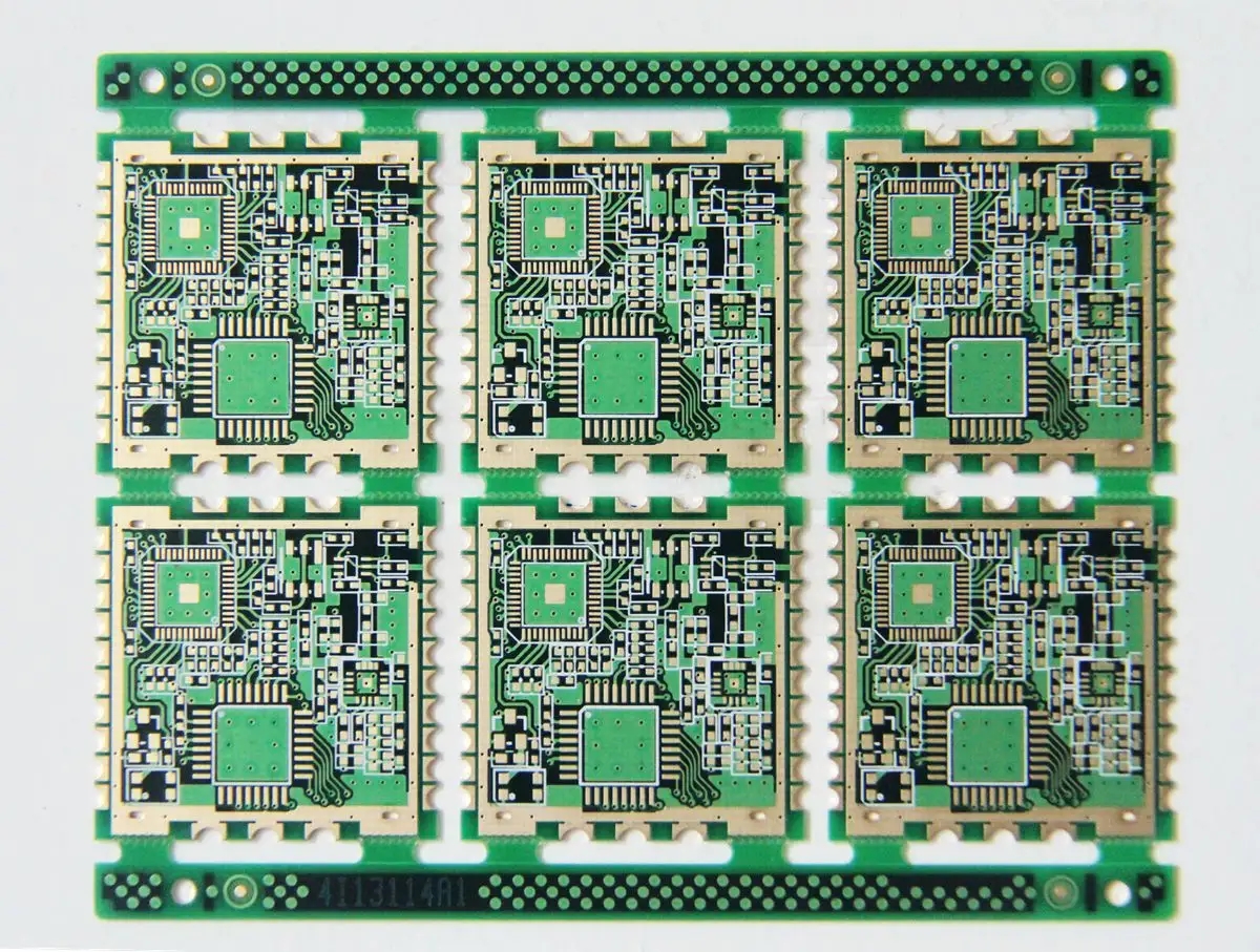
Four problems in PCBA chip processing
The systematic quality control details of solder paste printing and reflow temperature control in SMT chip processing are key nodes in the PCBA manufacturing process. At the same time, for the printing of high-precision circuit boards with special and complex processes, it is necessary to use laser steel mesh according to specific conditions to meet the circuit boards with higher quality requirements and more demanding processing requirements. According to PCB manufacturing requirements and customer product characteristics, some may need to add U-shaped holes or reduce steel mesh holes. The steel mesh shall be processed according to the requirements of PCBA processing technology.
1、 SMT chip assembly
The systematic quality control details of solder paste printing and reflow temperature control in SMT chip processing are key nodes in the PCBA manufacturing process. At the same time, for the printing of high-precision circuit boards with special and complex processes, it is necessary to use laser steel mesh according to specific conditions to meet the circuit boards with higher quality requirements and more demanding processing requirements. According to PCB manufacturing requirements and customer product characteristics, some may need to add U-shaped holes or reduce steel mesh holes. The steel mesh shall be processed according to the requirements of PCBA processing technology.
Four problems in PCBA chip processing
The temperature control accuracy of reflow soldering furnace is critical to the wetting of solder paste and the firmness of steel mesh welding, which can be adjusted according to the normal SOP operation guidelines. To minimize the quality defects of PCBA chip processing in the SMT link. In addition, strict implementation of AOI testing can greatly reduce defects caused by human factors.
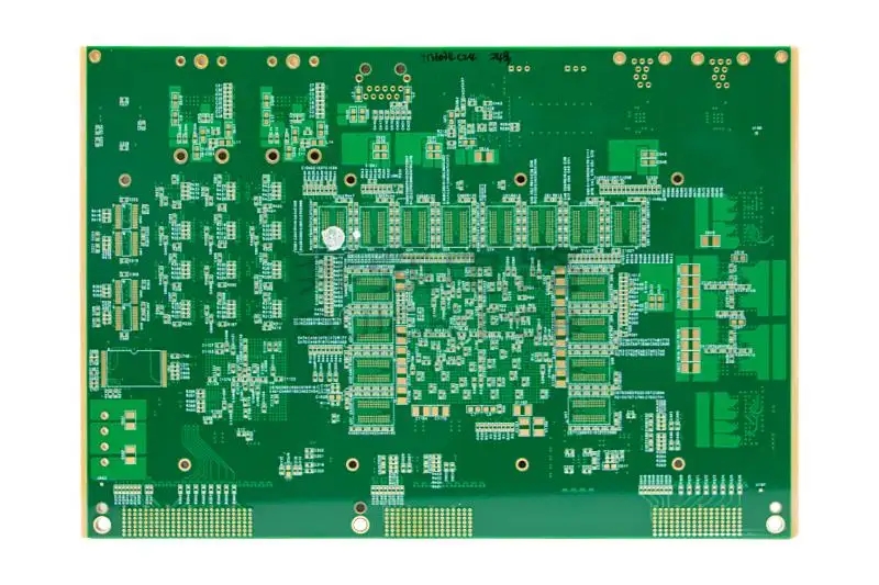
2、 DIP plug-in post welding
Post soldering of DIP plug-in is the most important and the last process of PCB processing. In the post welding process of DIP plug-in, it is very important to consider the furnace pass fixture for wave soldering. How to make use of furnace jigs to greatly improve the rate of qualified products and reduce poor soldering such as continuous tin, little tin and lack of tin. According to the different requirements of customers' products, pcba processing plants must constantly summarize experience in practice and achieve technical upgrading in the process of experience accumulation.
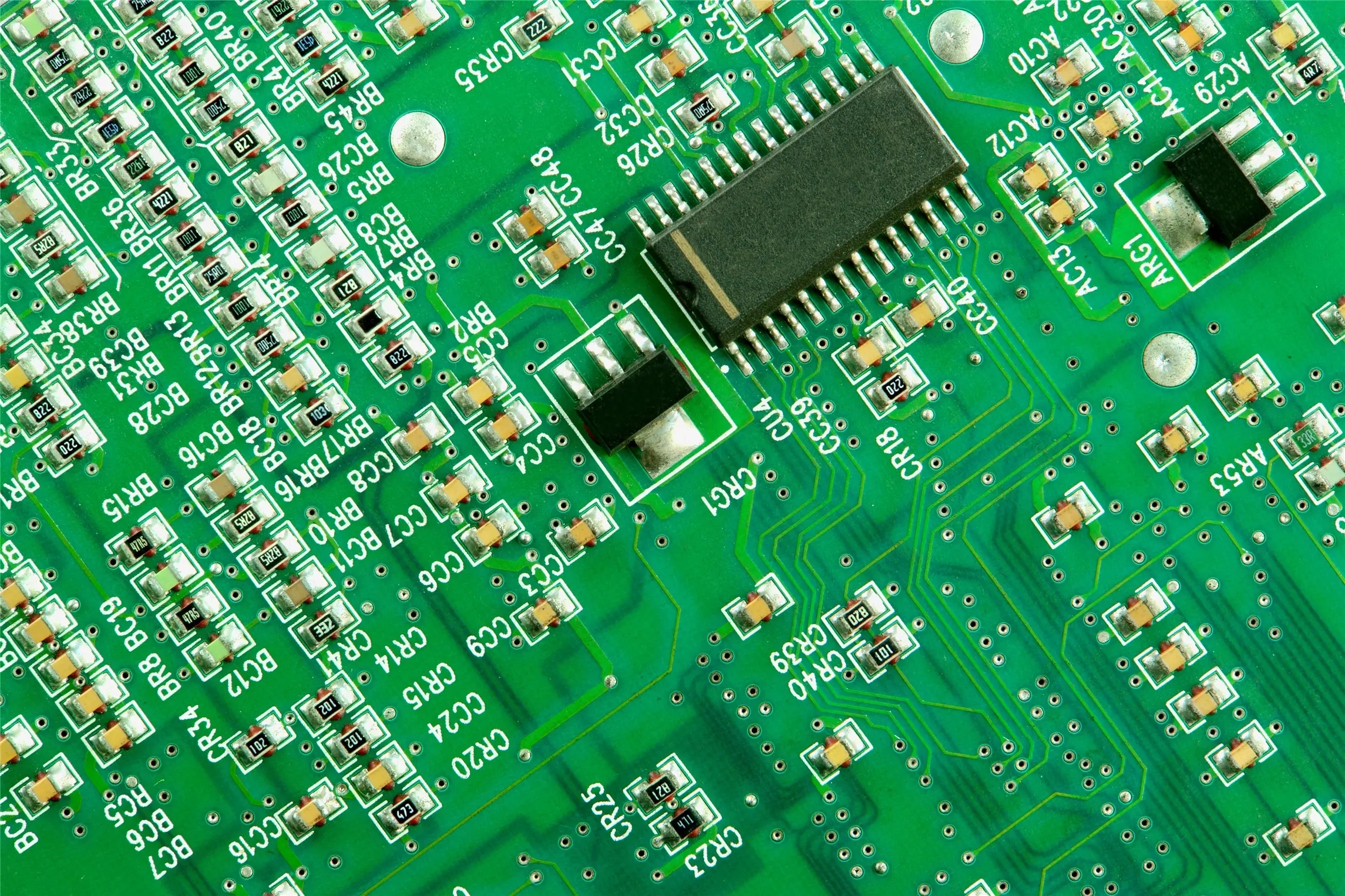
3、 Testing and procedure firing
The manufacturability report is an evaluation work that we should do before the whole production after receiving the production contract from the customer. In the early DFM report, we can provide some suggestions to the customer before PCB processing, such as setting some key test points on PCB (test points), so as to conduct PCB welding test and subsequent key tests on circuit continuity and connectivity after PCBA processing. When conditions permit, you can communicate with the customer to provide the back-end program, and then burn the PCBA program to the core master IC through the burner. In this way, the circuit board can be tested more concisely through touch action, so as to test and inspect the integrity of the entire PCBA and find defective products in time.
4、 PCBA manufacturing test
In addition, many customers who seek the one-stop service of PCBA processing also have requirements for the back-end testing of PCBA. This test generally includes ICT (circuit test), FCT (function test), burn test (aging test), temperature and humidity test, drop test, etc.


Just upload Gerber files, BOM files and design files, and the KINGFORD team will provide a complete quotation within 24h.