
Professional PCB manufacturing and assembly
Building 6, Zone 3, Yuekang Road,Bao'an District, Shenzhen, China
+86-13410863085Mon.-Sat.08:00-20:00

How to reduce and eliminate solder beads and dross on PCBA board?
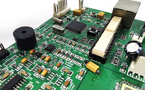
In the PCBA processing process, due to the factors of process and manual operation, there is a high probability that the occasional tin bead and tin slag will inevitably remain on the PCBA board, which will cause great hidden danger to the use of the product. Because the tin bead and tin slag will become loose in an uncertain environment, forming a short circuit on the PCBA board, resulting in product failure. The key is that this probability of occurrence is likely to occur in the life cycle of the product, which will exert great pressure on the after-sales of customers.
The Basic Cause of PCBA Tin Beads and Slags
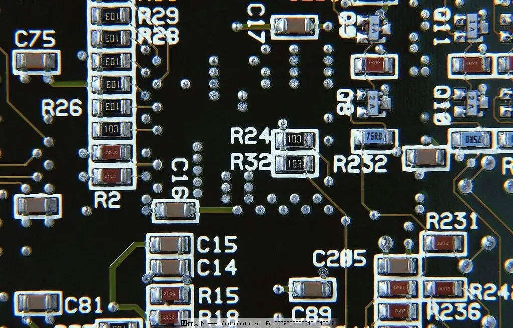
1. There is too much tin on the SMD pad. During the reflow soldering process, the corresponding tin beads are extruded from the molten tin
2. PCB board or components are affected with moisture, moisture will burst during reflow soldering, and the spattered tin beads will fall on the board surface
3. During DIP plug-in post soldering operation, when manually adding tin and throwing tin, the tin beads splashed by the soldering iron head scattered on the PCBA board
4. Other unknown reasons
Measures for Reducing PCBA Tin Beads and Slags
1. Attention should be paid to the fabrication of stencil, and the opening size should be properly adjusted according to the specific component layout of PCBA board, so as to control the printing amount of solder paste. Especially for some tight pin components or board components which are dense.
2. For bare PCB boards with BGA, QFN and foot tight components on the board surface, strict baking action is recommended to ensure the removal of moisture on the pad surface, maximize solderability and eliminate solder beads
3. PCBA manufacturers will inevitably introduce manual welding stations, which requires strict control of tin throwing operation in management. Arrange a special storage box, clean the table in time, and strengthen the visual inspection of SMD components around the manually welded components by the post welding QC, focusing on whether SMD component solder joints are accidentally touched and dissolved or solder beads and dross are scattered between component pins
PCBA board is a relatively precise product component, which is very sensitive to conductive objects and ESD static electricity. In the PCBA processing process, the factory managers need to improve the management level, strengthen the quality awareness of the operators and the quality team, implement from two aspects of process control and ideological awareness, and avoid the production of solder beads and dross on the PCBA board to the greatest extent.


Just upload Gerber files, BOM files and design files, and the KINGFORD team will provide a complete quotation within 24h.