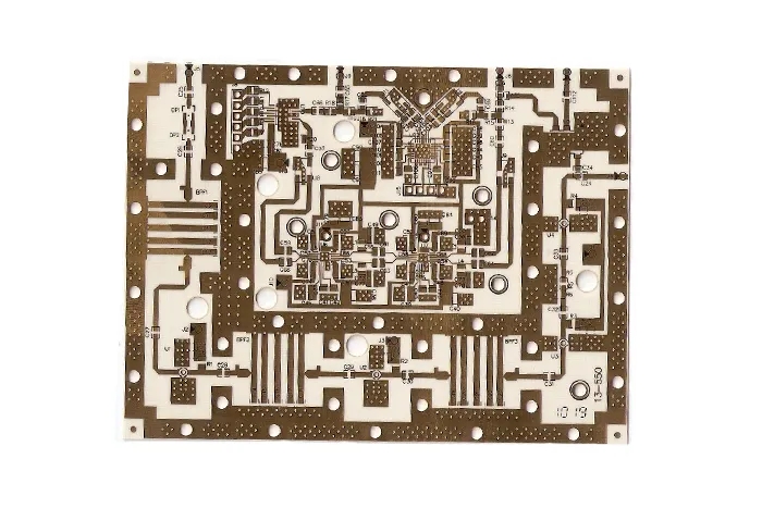
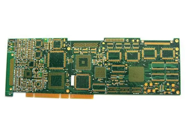
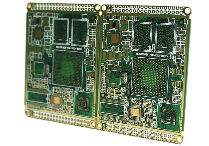
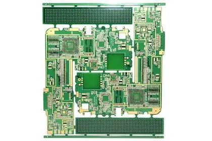
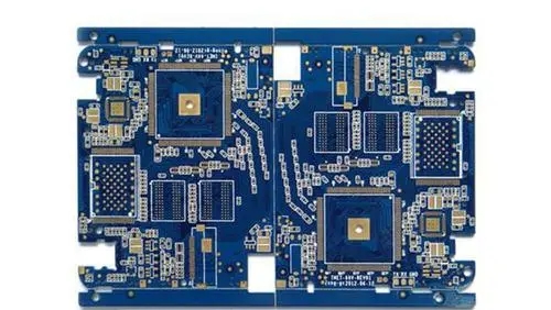
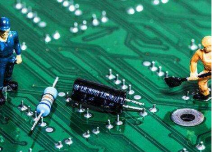
What is a double-layer circuit board_ How to draw double-layer and four layer PCB
PCB manufacturers, PCB designers and PCBA manufacturers will explain to you what a double-layer PCB ...


PCB manufacturers, PCB designers and PCBA manufacturers will explain to you what a double-layer PCB ...
Circuit board manufacturing, circuit board design and PCBA processing manufacturers will explain to ...
Circuit board manufacturing, circuit board design, PCBA processing manufacturers explain to you elec...
PCB manufacturing, PCB design and PCBA processing manufacturers will explain the PCB surface treatme...
PCB manufacturers, PCB designers and PCBA manufacturers explain the application and significance of ...
PCB manufacturers, PCB designers and PCBA manufacturers will explain the functions, requirements, pr...
PCB manufacturers, PCB designers and PCBA manufacturers explain to you: Do you know how PCB is produ...
Circuit board manufacturing, circuit board design and PCBA processing manufacturers explain electron...

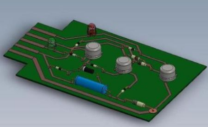
Understand PCB design, PCB layout and PCB manufacturing in PCB related industries and Let's see how ...
Understand PCB design, PCB layout and PCB manufacturing in PCB related industries and Explain and co...
Understand PCB design, PCB layout and PCB manufacturing in PCB related industries and Line descripti...
Understand PCB design, PCB layout and PCB manufacturing in PCB related industries and Look at the mo...
