
Professional PCB manufacturing and assembly
Building 6, Zone 3, Yuekang Road,Bao'an District, Shenzhen, China
+86-13410863085Mon.-Sat.08:00-20:00

What is a double-layer circuit board_ How to draw double-layer and four layer PCB
PCB manufacturers, PCB designers and PCBA manufacturers will explain to you what a double-layer PCB is_ How to draw double-layer and four layer PCB
Circuit board overview
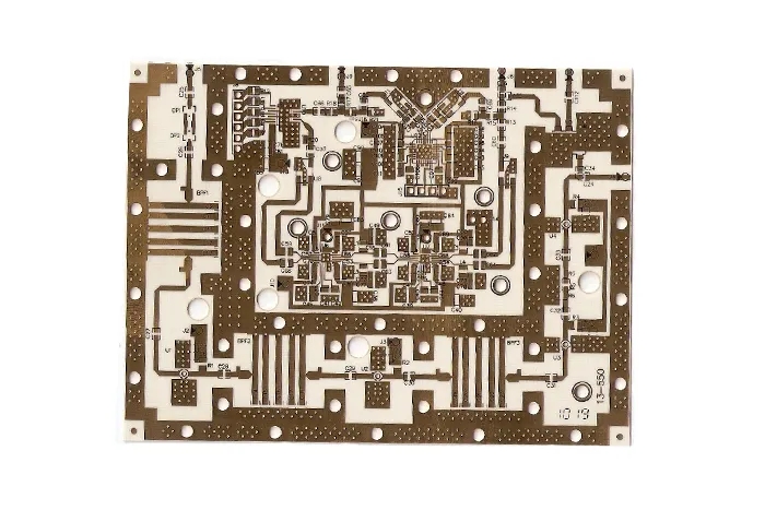
The names of circuit boards include: ceramic circuit board, alumina ceramic circuit board, aluminum nitride ceramic circuit board, circuit board, PCB board, aluminum substrate, high-frequency board, thick copper plate, impedance board, PCB, ultra-thin circuit board, ultra-thin circuit board, printed (copper etching technology) circuit board, etc. The circuit board makes the circuit miniature and intuitive, which plays an important role in the mass production of fixed circuits and the optimization of the layout of electrical appliances. The circuit board can be called printed circuit board or printed circuit board, and the English name is printed circuit board (PCB), flexible printed circuit board (FPC circuit board is also called flexible circuit board) FPC circuit board (FPC circuit board is a highly reliable and excellent flexible printed circuit board made of polyimide or polyester film as the substrate. It has the characteristics of high wiring density, light weight, thin thickness and good bending.) The birth and development of FPC and PCB (reechas, Soft hard combinaTIon plate) gave birth to this new product. Therefore, the soft and hard combination board is a circuit board with FPC characteristics and PCB characteristics formed by combining the flexible circuit board and the hard circuit board according to relevant process requirements after pressing and other processes.
Classification of circuit boards
According to the number of layers, PCB can be divided into single panel, double panel, and multi-layer PCB.
First is the single panel. On the Z basic PCB, the parts are concentrated on one side and the wires are concentrated on the other side. Because wires only appear on one side, this PCB is called single-sided circuit board. Single panel is usually simple to make and low in cost, but its disadvantage is that it cannot be applied to too complex products.
Double panel is an extension of single panel. When single-layer wiring cannot meet the needs of electronic products, double-sided panel will be used. Both sides are copper coated and wired, and the line between the two layers can be conducted through the via to form the required network connection.
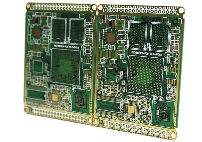
Multilayer board refers to a printed board with more than three conductive graphic layers and insulating materials between them laminated at intervals, and the conductive graphics between them are interconnected as required. Multilayer circuit board (MLPCB) is the product of the development of electronic information technology in the direction of high speed, multi-function, large capacity, small volume, thin and lightweight.
PCB can be divided into soft board (FPC), hard board (PCB) and soft hard combination board (FPCB) according to characteristics.
What is a double-layer circuit board
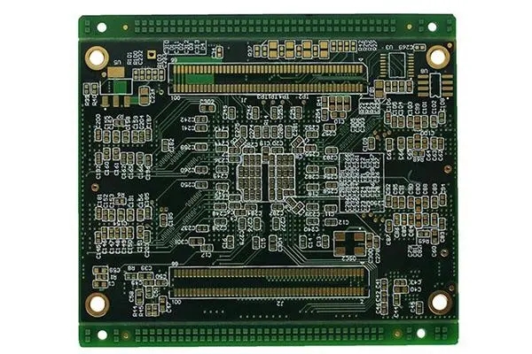
A PCB board has two sides, the top and bottom. This is the double-layer circuit board. Double layer circuit board is a PCB board with copper coating on both sides. Both sides of the double-layer circuit board are copper coated and wired, and the circuit between the two layers can be conducted through the via to form the required network connection.
Double layer PCB drawing
Steps for drawing double-layer pcb board:
1. Prepare the circuit schematic diagram
2. Create a PCB file and load it into the component packaging library
3. Planning circuit board
4. Load Network Tables and Components
5. Automatic layout of components
6. Layout adjustment
7. Network density analysis
8. Routing Rule Settings
9. Automatic routing
10. Manually adjust routing
Example of drawing double-layer PCB board:
Common EDA circuit software can design multilayer PCB circuit board. Although the methods are different, the principle is the same.
For PCB design, AD provides detailed 10 different design rules, including wire placement, wire routing method, component placement, routing rules, component movement and signal integrity rules. According to these rules, ProtelDXP performs automatic layout and automatic routing. To a large extent, the success of cabling and the quality of cabling depend on the reasonableness of design rules and the design experience of users.
Different design rules can be used for specific circuits. For double-sided boards, many rules can use the system default value. The system default value is the setting of wiring for double-sided boards.
Here we share the setting steps of a four layer PCB, and the 8-layer PCB and other multilayer boards are all set in this way. Other versions of AD are similar to this operation.
First, create a PCB file. If you have your own project, you can create it under your own project.
Select File New PCB
It can be seen that the built PCB has only two layers, TopLayer and BottomLayer..
Turn on cascading management. Design LayerStackManager, enter the cascading management interface.
You can see that there are only two layers: TopLayer and BottomLayer. You can see the AddLayer option on the right.
Click Add Layer twice to add two layers.
Double click the added layer name to modify it.
After modification, confirm. We can see that the four layers of PCB are set, GND and VCC layers are added, and the compiled schematic can be imported to draw the four layers of PCB.
The operation skills of each layer are the same as those of the single panel, but they need to be considered as a whole when designing.
How to draw a four layer PCB
1. First, create a PCB file. If you have your own project, you can create it under your own project.
Select File New PCB
2. It can be seen that the built PCB has only two layers, Top Layer and Bottom Layer.
3. Turn on cascading management. Design Layer Stack Manager, enter the cascading management interface.
You can see that there are only two layers: Top Layer and Bottom Layer. You can see the Add Layer option on the right.
4. Click Add Layer twice to Add two layers
5. Double click the added layer name to modify it
6. After the modification, confirm that we can see that the four layers of PCB are set, GND and VCC layers are added, and the compiled schematic can be imported to draw the four layers of PCB. PCB manufacturers, PCB designers and PCBA manufacturers will explain to you what a double-layer PCB is_ How to draw double-layer and four layer PCB.


Just upload Gerber files, BOM files and design files, and the KINGFORD team will provide a complete quotation within 24h.