
Professional PCB manufacturing and assembly
Building 6, Zone 3, Yuekang Road,Bao'an District, Shenzhen, China
+86-13410863085Mon.-Sat.08:00-20:00

Electronic engineer: What's the difference between PCB and IC?
Circuit board manufacturing, circuit board design and PCBA processing manufacturers will explain to you electronic engineers: What is the difference between PCB and integrated circuit?
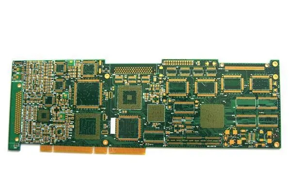
Composition of PCB
Current circuit boards are mainly composed of the following:
Line and pattern: The line is used as a tool for conducting between the original parts. In the design, a large copper surface will be additionally designed as the grounding and power supply layer. Lines and drawings are made at the same time.
Dielectric layer: It is used to maintain the insulation between lines and layers, commonly known as substrate.
Hole (Through hole/via): Through hole can make more than two layers of lines conductive to each other. The larger through hole is used as part plug-in. In addition, non through hole (nPTH) is usually used for surface mounting and positioning, and is used to fix screws during assembly.
Solder resistant/Solder Mask: Not all copper surfaces need tin coated parts. Therefore, non tin coated areas will be printed with a layer of substance (usually epoxy resin) to isolate tin on copper surfaces, so as to avoid short circuit between non tin coated lines. According to different processes, it can be divided into green oil, red oil and blue oil.
Legend/Marking/Silk screen: This is an unnecessary composition. Its main function is to mark the name and position box of each part on the circuit board for maintenance and identification after assembly.
Surface Finish: Since the copper surface is easy to oxidize in general environment, which leads to tin coating failure (poor solderability), it will be protected on the copper surface that needs tin. The protection methods include HASL, ENIG, Immersion Silver, Immersion Tin, and OSP. Each method has its advantages and disadvantages, which are collectively referred to as surface treatment.
PCB board characteristics
It can be high-density. For decades, the high density of printed boards has been developing with the improvement of integrated circuit integration and installation technology.
High reliability. Through a series of inspections, tests and aging tests, the PCB can be guaranteed to work reliably for a long time (service life, generally 20 years).
Designability. For various performance requirements of PCB (electrical, physical, chemical, mechanical, etc.), PCB design can be realized through design standardization, normalization, etc., with short time and high efficiency.
Producibility. With modern management, standardization, scale (quantity), automation and other production can be carried out to ensure product quality consistency.
Testability. A relatively complete test method, test standard, various test equipment and instruments have been established to test and identify the qualification and service life of PCB products.
Assemblability. PCB products are not only convenient for standardized assembly of various components, but also can be used for automatic and large-scale batch production. At the same time, PCB and various component assembly parts can also be assembled to form larger parts and systems, up to the whole machine.
Maintainability. Because PCB products and various component assembly parts are designed and produced in a standardized way, these parts are also standardized. Therefore, once the system fails, it can be replaced quickly, conveniently and flexibly, and the system can be recovered quickly. Of course, we can give more examples. Such as miniaturization, lightweight, high-speed signal transmission, etc.
Integrated circuit characteristics
Integrated circuit has the advantages of small size, light weight, few outgoing lines and welding points, long service life, high reliability, good performance, low cost and convenient for large-scale production. It is not only widely used in industrial and civil electronic equipment such as radio recorders, televisions, computers, etc., but also widely used in military, communications, remote control, etc. The assembly density of electronic equipment assembled with integrated circuits can be tens to thousands of times higher than that of transistors, and the stable working time of equipment can also be greatly improved.
Application examples of integrated circuits
1. 555 touch timing switch
The integrated circuit IC1 is a 555 timing circuit, which is connected here as a monostable circuit. At ordinary times, because there is no inductive voltage at the P terminal of the touch pad, the discharge of capacitor C1 is completed through pin 7 of 555, the output of pin 3 is low, the relay KS is released, and the electric light is not on.
When it is necessary to turn on the light, touch the metal sheet P with your hand, and the clutter signal voltage induced by the human body is increased from C2 to the trigger terminal of 555, so that the output of 555 changes from low to high, the relay KS is pulled in, and the electric light is turned on. At the same time, the seventh pin of 555 is cut off internally, and the power supply will charge C1 through R1, which is the start of timing.
When the voltage on capacitor C1 rises to 2/3 of the power supply voltage, the seventh pin of 555 turns on to discharge C1, and the output of the third pin changes from high level to low level. The relay releases, the light goes out, and the timing ends.
The timing length is determined by R1 and C1: T1=1.1R1 * C1.
2. Single power supply to dual power supply circuit
In the circuit of the figure, the time base circuit 555 is connected to a non steady state circuit, and the three pins output a square wave with a frequency of 20KHz and a duty cycle of 1:1. Pin 3 is high level, C4 is charged; At low level, C3 is charged. Due to the existence of VD1 and VD2, C3 and C4 are only charged but not discharged in the circuit. The charging value is EC. Connect the B terminal to the ground, and a+/- EC dual power supply is obtained at both ends of A and C. The output current of this circuit exceeds 50mA.
Differences between PCB board and integrated circuit
Integrated circuit generally refers to the integration of chips. For example, the Beiqiao chip on the motherboard and the CPU are all called integrated circuits, and the original name is also called integrated block. The printed circuit refers to the circuit board we usually see, as well as the printed soldering chip on the circuit board.
Integrated circuit (IC) is welded on PCB board; PCB board is the carrier of integrated circuit (IC). A PCB is a printed circuit board (PCB). Printed circuit board will appear in almost every kind of electronic equipment. If there are electronic parts in a certain device, the printed circuit board is embedded on PCB of different sizes. In addition to fixing various small parts, the main function of the printed circuit board is to electrically connect the upper parts.
To put it simply, integrated circuit is to integrate a general circuit into a chip. It is a whole. Once it is damaged internally, the chip will also be damaged. PCB can weld components by itself, and components can be replaced if they are damaged. Circuit board manufacturing, circuit board design and PCBA processing manufacturers will explain to you electronic engineers: What is the difference between PCB and integrated circuit?


Just upload Gerber files, BOM files and design files, and the KINGFORD team will provide a complete quotation within 24h.