
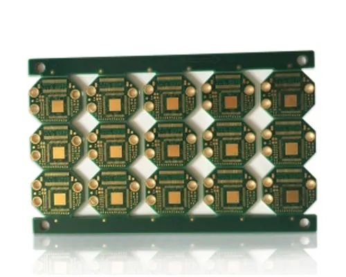
Professional PCB manufacturing and assembly
Building 6, Zone 3, Yuekang Road,Bao'an District, Shenzhen, China
+86-13410863085Mon.-Sat.08:00-20:00

Plug hole function, requirements and process of PCB design
PCB manufacturers, PCB designers and PCBA manufacturers will explain the functions, requirements, processes, advantages and disadvantages of the plug holes in PCB design
The conductive hole Via hole is also called conductive hole. In order to meet the customer's requirements, the conductive hole must be plugged. After a lot of practice, the traditional aluminum sheet plugging process has been changed, and the plate surface resistance welding and plugging are completed with white mesh. Stable production and reliable quality.
Via hole plays the role of connecting and conducting lines. The development of the electronic industry also promotes the development of PCB, and puts forward higher requirements for PCB manufacturing process and surface mounting technology. Via hole plug technology emerged as the times require, and the following requirements shall be met:
(1) Copper in the through hole can be used, but plug can be used for resistance welding;
(2) There must be tin lead in the through hole, with a certain thickness requirement (4 microns). Solder blocking ink is not allowed to enter the hole, causing tin beads to be hidden in the hole;
(3) The through hole must be provided with solder blocking ink plug hole, which is light tight, without tin ring, tin bead, flatness and other requirements. One side must be covered with oil, and the other side must be coated with Sn/Pb. Tin beads and tin rings are allowed

With the development of electronic products in the direction of "light, thin, short and small", PCB is also developing towards high density and high difficulty, so a large number of SMT and BGA PCBs appear. Customers require plug holes when mounting components, which have five main functions:
(1) Prevent short circuit caused by tin penetrating the component surface from the through hole during PCB over wave soldering;
(2) Avoid flux residues in the through hole;
(3) After the surface mounting and component assembly of the electronics factory are completed, the PCB must be vacuumed on the testing machine to form a negative pressure:
(4) Prevent the solder paste on the surface from flowing into the hole, causing false soldering and affecting the mounting;
(5) Prevent solder beads from popping up during wave soldering, causing short circuit.
Circuit Board Plug Hole Process and Its Advantages and Disadvantages
For surface mounting plates, especially BGA and IC mounting, the through hole plug hole must be flat, plus or minus 1 MIL convex and concave, and there must be no red tin on the edge of the through hole; In order to meet the customer's requirements, the through hole plug hole process can be described as varied, the process flow is particularly long, and it is difficult to control the process. Oil is often lost during hot air leveling and green oil solder resistance test; Oil explosion and other problems occur after curing. According to the actual production conditions, this paper summarizes various PCB plug hole processes, and makes some comparisons and explanations in the process, advantages and disadvantages:
I. Hot air leveling and plug hole process
The process flow is: resistance welding of plate surface → HAL → plug hole → curing. Non plug hole process shall be adopted for production. After hot air leveling, aluminum screen or ink screen shall be used to complete the through hole plug holes of all fortresses required by customers. The hole stopper ink can be photosensitive ink or thermosetting ink. Under the condition that the wet film color is consistent, the hole stopper ink is better to use the same ink as the board surface. This process flow can ensure that the through hole will not lose oil after hot air leveling, but it is easy to cause the ink of the plug hole to pollute the board surface and be uneven. The customer is easy to cause faulty soldering (especially in BGA) during mounting. Therefore, many customers do not accept this method.
Second hot air leveling front plug hole process
2.1 Use aluminum sheet to plug holes, solidify and grind plates, and then transfer graphics. In this process, use a numerical control drilling machine to drill aluminum sheets that need to be plugged, make them into screen plates, and plug holes to ensure that the through hole plug holes are full. The hole plug ink can also be used as thermosetting ink. Its characteristics must be high hardness, small resin shrinkage change, and good adhesion with the hole wall. The process flow is: pretreatment → plug hole → plate grinding → pattern transfer → etching → plate surface resistance welding
This method can ensure that the plug hole of the through hole is flat, and the hot air leveling will not have quality problems such as oil explosion and oil loss at the hole edge. However, this process requires one-time thickening of the copper to make the copper thickness of the hole wall meet the customer's standards. Therefore, there are high requirements for the copper plating of the whole plate, and there are also high requirements for the performance of the grinder to ensure that the resin on the copper surface is completely removed, and the copper surface is clean and not polluted. Many PCB plants do not have a one-time copper thickening process, and the performance of the equipment does not meet the requirements, resulting in less use of this process in PCB plants.
2.2 Resistance welding of direct screen plate surface after aluminum sheet plug hole
In this process, a CNC drilling machine is used to drill the aluminum sheet that needs to be plugged into a screen, which is installed on a silk screen machine to plug the hole. After the hole is plugged, the machine shall be parked for no more than 30 minutes. The 36T screen is used to directly screen the surface of the plate for resistance welding. The process flow is: pre-treatment -- plug hole -- silk screen -- pre drying -- exposure -- development -- curing
With this process, it can ensure that the through hole cover oil is good, the plug hole is flat, and the wet film color is consistent. After the hot air leveling, it can ensure that the through hole of PCB board is not tinned, and there is no tin bead in the hole, but it is easy to cause the ink on the pad in the hole after curing, resulting in poor solderability; After the hot air is leveled, the edge of the through hole bubbles and loses oil. It is difficult to control the production with this process method. The process engineer must adopt special processes and parameters to ensure the quality of the plug hole.
2.3 Aluminum sheet plug hole, development, pre curing, plate surface resistance welding after grinding.
Use a numerical control drilling machine to drill the aluminum sheet that requires a plug hole, make it into a screen plate, and install it on the displacement screen printing machine for the plug hole. The plug hole must be full, and the two sides are preferred to protrude. Then, after curing, grind the plate for surface treatment. The process flow is: pre-treatment -- plug hole -- pre drying -- development -- pre curing -- plate surface resistance welding
Because this process uses the plug hole curing to ensure that the oil will not drop or explode after HAL, but after HAL, it is difficult to completely solve the problem of tin coating on the through hole tin bead and through hole, so many customers do not accept it.
2.4 The plate surface resistance welding and plug hole shall be completed at the same time.
This method uses 36T (43T) screen, which is installed on the screen printing machine, and uses a backing plate or a nail bed. While completing the board surface, all the through holes are plugged. The process flow is: pretreatment -- screen printing -- pre drying -- exposure -- development -- curing
This process has a short time and a high utilization rate of equipment, which can ensure that no oil will fall from the vias and no tin will be added to the through holes after hot air leveling. However, due to the use of silk screen to plug holes, there is a large amount of air in the vias. When curing, the air expands and breaks through the solder mask, causing holes and irregularities. A small amount of tin will be hidden in the through holes after hot air leveling. At present, after a lot of experiments, our company has basically solved the problem of vias and unevenness by selecting different types of inks and viscosities, adjusting the pressure of silk screen, etc., and has adopted this process for batch production. PCB manufacturers, PCB designers, and PCBA manufacturers will explain the functions, requirements, processes, advantages and disadvantages of the plug holes in PCB design.


Just upload Gerber files, BOM files and design files, and the KINGFORD team will provide a complete quotation within 24h.