
Professional PCB manufacturing and assembly
Building 6, Zone 3, Yuekang Road,Bao'an District, Shenzhen, China
+86-13410863085Mon.-Sat.08:00-20:00

What are the components of a circuit board?
The names of circuit boards include: ceramic circuit board, alumina ceramic circuit board, aluminum nitride ceramic circuit board, circuit board, PCB board, aluminum substrate, high-frequency board, thick copper plate, impedance board, PCB, ultra-thin circuit board, ultra-thin circuit board, printed (copper etching technology) circuit board, etc. The circuit board makes the circuit miniature and intuitive, which plays an important role in the mass production of fixed circuits and the optimization of the layout of electrical appliances. The circuit board can be called printed circuit board or printed circuit board, and the English name is printed circuit board (PCB), flexible printed circuit board (FPC circuit board is also called flexible circuit board) FPC circuit board (FPC circuit board is a highly reliable and excellent flexible printed circuit board made of polyimide or polyester film as the substrate. It has the characteristics of high wiring density, light weight, thin thickness and good bending.) The birth and development of FPC and PCB (reechas, Soft and hard combination plate) gave birth to this new product. Therefore, the soft and hard combination board is a circuit board with FPC characteristics and PCB characteristics formed by combining the flexible circuit board and the hard circuit board according to relevant process requirements after pressing and other processes.
According to the number of layers, PCB can be divided into single panel, double panel, and multi-layer PCB.
First is the single panel. On the most basic PCB, parts are concentrated on one side and wires are concentrated on the other side. Because wires only appear on one side, this PCB is called single-sided circuit board. Single panel is usually simple to make and low in cost, but its disadvantage is that it cannot be applied to too complex products.
Double panel is an extension of single panel. When single-layer wiring cannot meet the needs of electronic products, double-sided panel will be used. Both sides are copper coated and wired, and the line between the two layers can be conducted through the via to form the required network connection.
Multilayer board refers to a printed board with more than three conductive graphic layers and insulating materials between them laminated at intervals, and the conductive graphics between them are interconnected as required. Multilayer circuit board (MLPCB) is the product of the development of electronic information technology in the direction of high speed, multi-function, large capacity, small volume, thin and lightweight.
PCB can be divided into soft board (FPC), hard board (PCB) and soft hard combination board (FPCB) according to characteristics.
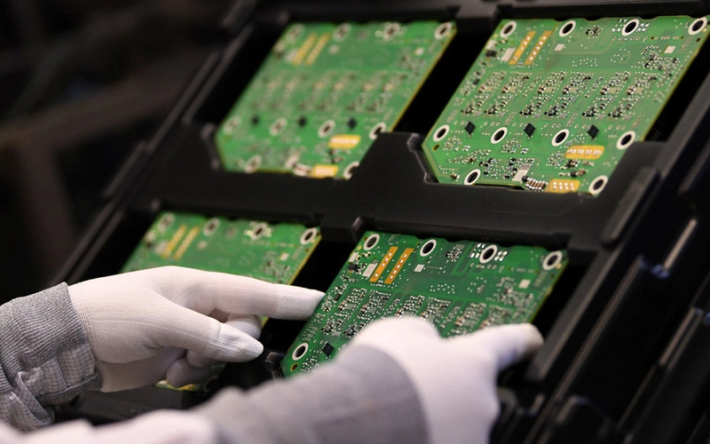
The era of interconnection of all things is full of intelligent electronic products. The circuit board is the core component of electronic products. Let's learn what the circuit board is composed of:
1. Pads:
A bonding pad is a metal hole used to weld the pins of components.
2. Layer:
According to different designs, circuit boards can have double-sided boards, 4-layer boards, 6-layer boards, 8-layer boards, etc. The number of layers is usually an even number. In addition to the layers that take signals, there are other layers used to define processing.
3. Through hole:
The meaning of vias is that if the circuit can not realize all signal wiring on one layer, the signal wires should be connected across layers through vias. There are two types of vias, one is metal vias, and the other is non-metal vias, where metal vias are used to connect the pins of components between layers. The form and diameter of the through hole depend on the characteristics of the signal and the process requirements of the processing plant.
4. Components:
For components welded on PCB, wiring combination between different components can realize different functions, which is also the role of PCB.
5. Routing:
The routing refers to the signal line between the pins of the connector. The length and width of the routing depends on the nature of the signal, such as the current size, speed, etc. The length and width of the routing are also different.
6. Silk screen:
Silk screen can also be called silk screen layer, which is used to mark various relevant information of devices. The silk screen is generally white, and the color can also be selected according to your own needs.
7. Solder resistance layer:
The main function of the solder mask is to protect the PCB surface, form a protective layer with a certain thickness, and block the contact between copper and air. The solder mask is generally green, but there are also red, yellow, blue, white and black solder mask options.
8. Locating hole:
The positioning hole is a hole for easy installation or commissioning.
9. Fill:
The filling is used for copper coating of ground wire network, which can effectively reduce the impedance.
10. Electrical boundary:
The electrical boundary is used to determine the size of the circuit board. All components on the circuit board cannot exceed the boundary.
The above ten parts are the basis of the circuit board, and more functions can be achieved only by burning programs in the chip.
PCBA circuit board maintenance post
Oct 27,2022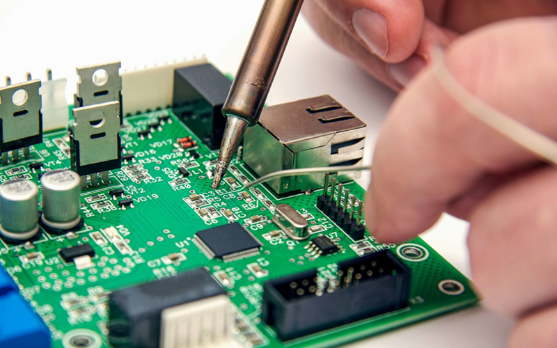


Just upload Gerber files, BOM files and design files, and the KINGFORD team will provide a complete quotation within 24h.