
Professional PCB manufacturing and assembly
Building 6, Zone 3, Yuekang Road,Bao'an District, Shenzhen, China
+86-13410863085Mon.-Sat.08:00-20:00

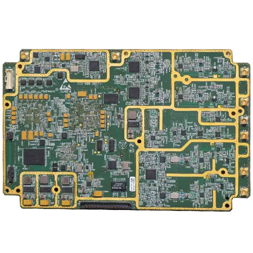
In PCB design, after completing the PCB design through many levels, the most important thing is the copyright issue, and plagiarism is common. So, how does PCB design prevent others from copying the board? Next, PCB design company -kingford Electronics introduces the way of PCB design anti-copying board.
1.Use fine sandpaper to remove the model number on the chip. More effective against a side-gate chip.
2. Sealing glue, such as adhesive steel, etc., will cover all the components above the PCB; Five or six flying wires can also be deliberately twisted together. It should be noted that the glue cannot be corroded, and the heat in the closed area will not be too large.
3. Use a dedicated encryption chip, such as ATMEL's AT88SC153.
4. Use an uncrackable chip, such as the EPM7128 or higher of the EPLD. ACTEL CPLD, etc.
5. Use MASKIC, which requires a lot of batch.
6. Using bare pieces, plagiarists cannot see the model and do not know the connection. But the chip's function is not too easy to guess.
7. Resistors above 60 ohms in series on signal lines with low current.
8. Use some small components without words (or only some code names) TO participate in signal processing, such as small chip capacitors, TO-XX diodes, etc.
9. Cross some addresses and data lines.
10. PCB adopts buried hole and blind hole technology, so that the hole is hidden in the board.
11. Use other special accessories, such as customized LCD screens, customized transformers, etc.
12. Apply for a patent. In view of the poor intellectual property protection environment, the best foreign approach can only be put in the last line.
Maximum signal design rate: 10Gbps CML differential signal;
Maximum PCB design layer: 40 layers;
Minimum line width: 2.4mil;
Minimum line spacing: 2.4mil;
Minimum BGA PIN spacing: 0.4mm;
Minimum mechanical hole diameter: 6mil;
Minimum laser drilling diameter: 4mil;
Maximum number of pins: 63000+
Maximum number of components: 3600;
Maximum number of BGA: 48+.
PCB design service flow
1.Customers provide schematics to consult PCB design;
2. Evaluate quotation according to schematic diagram and customer design requirements;
3. The customer confirms the quotation, signs the contract, and prepays the project deposit;
4. Received advance payment and arranged engineer design;
5. After the design is completed, provide the screenshot of the document to the customer for confirmation;
6. The customer confirmed OK, settled the balance, and provided PCB design information.


Just upload Gerber files, BOM files and design files, and the KINGFORD team will provide a complete quotation within 24h.