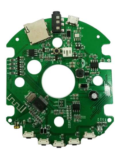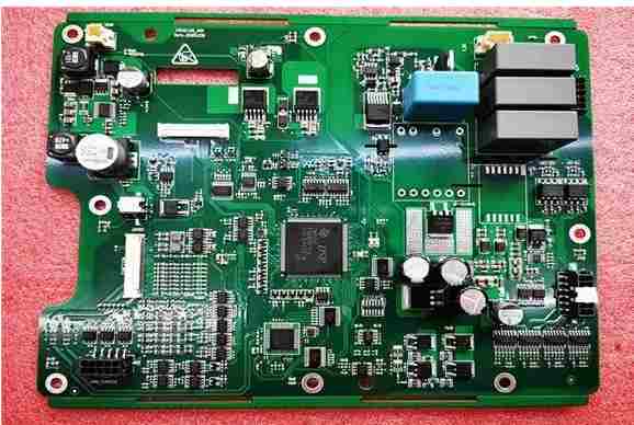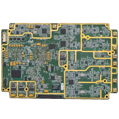
PCB design technology is very complex, involving a lot of problems in all aspects, to do a good job of PCB design requires the accumulation of experience, professional PCB design for more than 20 years, next for everyone to share the eight common technical problems of PCB design.
1, Design a system containing DSP, PLD, from which aspects to consider ESD?
In terms of the general system, the main consideration is the direct contact of the human body, and the appropriate protection is carried out on the circuit and the mechanism. How much impact ESD will have on the system depends on different situations.
2, What aspects should be paid attention to in the design to suppress electromagnetic radiation?
A: The three elements of EMC are radiation source, transmission path and victim; The transmission ways are divided into space radiation transmission and cable conduction. So to suppress harmonics, first look at the way it spreads. Power decoupling is the solution to conductive mode propagation, in addition, the necessary matching and shielding are also required.

3, the use of 4-layer board design products, why are some surface paving, some are not?
A: The role of paving:
shielding;
heat dissipation;
reinforcement;
process processing needs. No matter how many layers of flooring, we must first look at its main reasons. Here we are mainly talking about high speed. Surface paving is good for EMC, but copper paving should be as complete as possible to avoid islands.
4, frequency more than 30M plate, the use of automatic wiring or manual wiring?
A: Automatic or manual wiring depends on the support of the software wiring function, some wiring may be better than automatic wiring, but some wiring, such as check wiring, bus delay compensation wiring, automatic wiring effect and efficiency will be much higher than manual wiring.
5, in the design, the ground is usually divided into protective ground and signal ground; Power ground is divided into digital ground and analog ground, why should the ground be divided?
A: The purpose of the division is mainly due to EMC considerations, worrying that the digital part of the power supply and the noise on the ground will interfere with other signals, especially analog signals through the transmission path. No matter how it is divided, there is only one final earth.
6, when the clock is distributed, is it necessary to add ground wire shielding on both sides?
A: Whether to add the shielding ground wire should be determined according to the crosstalk /EMI situation on the board, if the shielding ground wire is not handled well, it may make the situation worse.
7. What are the corresponding countermeasures for distributing clock lines of different frequencies?
A: For the wiring of the clock line, it is best to carry out signal integrity analysis, formulate corresponding wiring rules, and perform wiring according to these rules.
8, single-layer plate manual wiring, how to represent the jumper?
A: The jumper is a special device in the design, only two pads, the distance can be fixed length, can also be variable length. Manual wiring can be added as needed. There will be a direct line on the PCBA board, and it will also appear in the material list.


