
Professional PCB manufacturing and assembly
Building 6, Zone 3, Yuekang Road,Bao'an District, Shenzhen, China
+86-13410863085Mon.-Sat.08:00-20:00

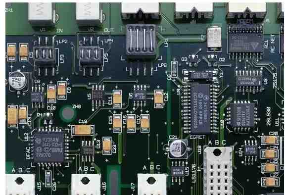
BOM is an abbreviation of English (Bill of Material), and Chinese means bill of materials. As the name implies, it is a list of all the materials used in the processing of a product. Therefore, the BOM list is very important for the SMT patch processing plant, which contains important information in the entire product processing process.
Since the BOM list provided by the customer is not perfect, the general SMT patch processing plant needs to be converted into the form of internal company files for issuance, so what are the precautions for SMT patch processing plants to sort out the BOM list? The following kingford one-stop PCBA manufacturers to talk about SMT patch BOM list arrangement precautions.
1, BOM list arrangement contents include: process, material code, material name, description, brand, bit number, dosage, remarks;
2,The components used in SMT patch processing and DIP plug-in processing are sorted and classified to facilitate each process in the production process at a glance;
3, the description must be clear, including model, package, resistance and capacitance value size;
4, there are some crucial electronic components, the customer hopes that the SMT patch factory in accordance with the designated brand to purchase. At the same time, considering the fluctuations of the component market and the cost, alternative models can be selected when necessary to make remarks;
5,Check whether the digit number and quantity of each item are consistent, and check whether the coordinate and digit number are completely coincident;

6, according to the coordinate T/B to distinguish the positive and negative coordinate values required. The SMT patch factory can sort out the standard BOM list, which is the benchmark to ensure the accuracy of product processing. Without a complete BOM, it is impossible to produce a PCBA with quality assurance, so the accuracy of the BOM is very important. Our own SMT processing plant can provide SMT processing services for minimum package 0201 components. Professional to provide overall PCBA electronic manufacturing services, including upstream electronic component procurement to PCB production and processing, SMT patches, DIP plug-ins, PCBA testing, finished product assembly and other one-stop services.
In PCB design, you may often hear the terms "through the hole window" and "through the hole cover oil". In fact, it is literally, one hole to open the window, one hole to cover the oil. In other words, whether to insulate the PCB surface means that it is easy to tin the position of the window, and it can be judged whether to open the window according to whether it can be tin. Cover oil, refers to the time when the patch is not easy to tin, which is determined by the process. The reasons why there is no oil covered through the hole are as follows: because the solder resistance oil is liquid and the middle of the hole is empty, it is easy for the solder resistance oil on the solder resistance ring to enter the hole during the roasting process, resulting in yellow through the hole. This situation is related to the concentration of welding oil, the oven and the application force, so there will be green on some of them. And then there are the ones that don't.
Why solder resistance window opening?
For the hole, if the window is not opened, the ink of the solder resistance layer will enter the hole. For some holes that do not need ink plugs, it is necessary to design it to open the window through the hole. For through-hole mounted components, if the PCB is not soldered to open the window, the components will not be welded to the board properly. Aperture opening window is not only convenient for welding, but also can be measured on the hole. For some special positions of the hole welding window, you can use a multimeter to measure on the hole.
For PCB, if the window is not opened, the surface treatment can not be carried out, and tin spraying and welding can not be carried out.
How to weld the window opening?
1,The welding pad will open the window by default in the PCB design (OVERRIDE: 0.1016mm), that is, the welding pad is exposed to copper foil, and the external expansion is 0.1016mm, and the wave soldering is tinned. It is recommended that no design changes be made to ensure weldability.
2, the hole will open the window by default in the PCB design (OVERRIDE: 0.1016mm), that is, the hole will expose the copper foil, the external expansion of 0.1016mm, and the tin will be tin during wave soldering. If designed to prevent tinning through the hole and not expose copper, you must check the PENTING option in the additional properties of the SOLDER MASK to close the through hole.
3, in addition, this layer can also be used alone for non-electrical wiring, then welding green oil corresponding window. If it is above the copper foil wire, it is used to enhance the current ability of the wire, and can be tinned when welding. If it is on a non-copper foil track, it is usually designed for logo and special character screen printing, which can save production.


Just upload Gerber files, BOM files and design files, and the KINGFORD team will provide a complete quotation within 24h.