
Professional PCB manufacturing and assembly
Building 6, Zone 3, Yuekang Road,Bao'an District, Shenzhen, China
+86-13410863085Mon.-Sat.08:00-20:00

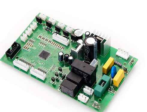
IC is the English abbreviation of integrated circuit IntegratedCircuit, the industry usually divides the type of IC according to the form of IC package, traditional IC has SOP, SOJ, QFP, PLCC, etc., relatively new IC has BGA, CSP, FLIPCHIP, etc. Due to the number of their pins (part pins) and the spacing between pins and pins, their shapes vary.The packaging form of chip components is one of the packaging forms of semiconductor devices, involving a wide variety of SMT processingSMT stick processingparts, a variety of styles, many have become a common standard in the industry, mainly some chip capacitors and resistors; Many are still changing, especially IC parts, and the changes in the packaging form are endless, which is dizzying.
")
Production, IC splicing is more difficult, after all, IC is generally a more needle number of IC, which requires our SMT chip processing personnel to be careful and patient to treat and strictly in accordance with the processing requirements to operate in order to get and machine stick quality equivalent products. Chip hand welding has many noteworthy places, such as due to the high degree of internal integration, affected by overheating is also easy to damage, the general SMT proof machine can not withstand the temperature of more than 200 ° C.
1.Welding time should be as short as possible, generally no more than 3s.
2. The electric soldering iron used is a constant temperature of 230 degrees.
3. The SMT proof machine workbench should be well anti-static treatment.
4. Choose a narrow tip of the soldering iron head, welding will not touch the adjacent endpoint.
5. In SMT chip processing, do not take out the pre-set short circuit before CMOS circuit welding.
6. The plug of the electroplating circuit can not be scraped off with a knife, just scrub with alcohol, or clean with a drawing eraser. Electronic Co., Ltd. is a professional PCBA OEM manufacturer, which can provide the overall PCBA electronic manufacturing services, including upstream electronic component procurement to PCB production and processing, SMT, DIP plug-in, PCBA testing, finished product assembly and other one-stop services.
The company gives full play to its competitive advantages in scale procurement and quality control, and has signed long-term cooperation agreements with many electronic component manufacturers at home and abroad and around the world to ensure the quality and stable supply of raw materials, and transfer the benefits to customers.
In the SMT patch processing, we generally use the automatic scrubbing method to remove. The mode of scrubbing is wet wipe, vacuum wipe and dry wipe, usually using the combination process of wet wipe/vacuum wipe, that is, wet wipe first, then vacuum wipe and dry wipe. The combination process of wet wipe and vacuum wipe can also be used. The purpose of wet rubbing is to remove residual solder paste from the bottom of the template, while the purpose of dry rubbing is to remove residual cleaning agent and flux from the bottom.
The vacuum wipe nominally hopes to absorb the residual solder paste in the opening of the printing template, but the actual effect depends on the proportion of the opening area of the template, and the possible effective function is to absorb the cleaning agent infiltrated into the hole wall, so as not to affect the first printing effect after the wipe. In the actual PCBA processing, in addition to the automatic cleaning function, it is also necessary to carry out regular manual cleaning. Because in the process of printing solder paste for a long time, the components at the bottom of the steel mesh will be contaminated, thus forming a hard scab around the mesh, and this kind of thing needs to be manually removed by the processing personnel on a regular basis.
Generally, after the artificial wet wipe, it should be dry wiped or placed for a few minutes, otherwise it may lead to the first one or two plates under the tin is not good. Because the manual wiping net is wet, too much cleaning agent penetrates into the opening hole wall, and the rapid volatilization of cleaning agent leads to an increase in the viscosity of the solder paste, which affects the solder under the SMT patch.
How to avoid printing faults in SMT processing?
Jun 19,2023


Just upload Gerber files, BOM files and design files, and the KINGFORD team will provide a complete quotation within 24h.