
Professional PCB manufacturing and assembly
Building 6, Zone 3, Yuekang Road,Bao'an District, Shenzhen, China
+86-13410863085Mon.-Sat.08:00-20:00

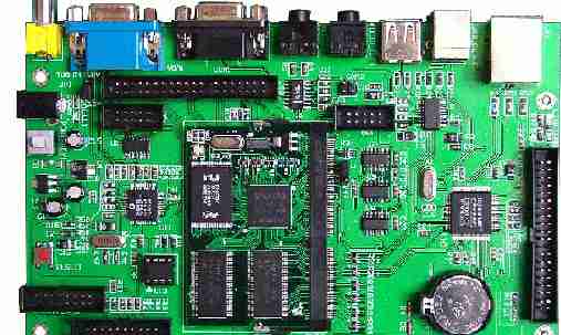
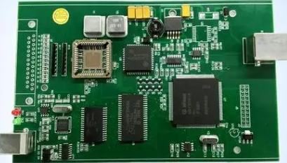
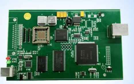
Surface Mount Technology (SMT) is a very important technology in the assembly process of electronic components, which is the method of attaching SMD components directly to the PCB board to realize the assembly of electronic components. The emergence of SMT technology has greatly improved the assembly efficiency and production quality of electronic components, and it has become an indispensable part of modern electronic production.
As a complex technology, there are many kinds of SMT processing processes. Can provide PCBA OEM one-stop service, next for you to introduce 4 common SMT processing process in detail.
")
1. Presequence preparation
Before SMT processing, the device and the board need to be processed. For components, it is necessary to carry out pre-preparation, including cleaning, stripping, processing, etc., to ensure that its quality meets the requirements. For PCB board, it is necessary to carry out the pre-preparation and treatment, including cutting, marking, layout, drilling, etc. After these treatments, the original and PCB board are ready, and then SMT processing can be carried out.
2. FeedFeeding refers to feeding the components prepared in the preceding sequence in accordance with fixed procedures. At this stage, components need to be classified according to specifications, sizes, models, etc., and placed in the process location. After the feeding is complete, check whether the placement of the components is correct.
Step 3 Print
Printing refers to the process of pasting SMD components on the PCB board after dispensing. The SMD component is fixed by dispensing glue on the PCB board. In the printing process, it is necessary to fine-adjust the parameters such as the thickness of the printing glue, the offset printing pressure, and the spacing of the scraper plate. After printing is completed, it is necessary to check the coverage area and uniformity of the glue.
Step 4 CureCuring is to fix the colloids on the PCB by heating the attached SMD components, so as to complete the component patch. In this link, it is necessary to regularly detect the temperature change of the metal makeup plate to ensure the correct process. After curing, it is necessary to test and check the fitting degree and mounting position of the components.
In short, the SMT processing process is a complex process that needs to complete several steps successively. Just completing one of the steps does not guarantee the quality of the processing, and requires comprehensive control. I believe that in the future of electronic production, SMT processing technology will continue to evolve and become more mature, and can bring greater help to our production.
1.Reasonably plan the thickness and composition of the copper layer
In high-speed PCB design, the thickness and composition of the copper layer have a very large impact on signal transmission. Therefore, we need to plan the copper layer before the design according to the design requirements. Generally speaking, when we lay copper, we can use the inner layer of copper and the outer layer of copper. The main function of the inner layer of copper is to provide an electrical connection for the PCB board, which can eliminate electromagnetic waves in the board by laying copper before signal transmission and improve signal stability. The outer layer of copper is mainly to improve the mechanical strength of the PCB board.
2. Use the appropriate copper laying method
In high-speed PCB design, we need to use a suitable copper paving method to ensure the stability of signal transmission. Generally speaking, we can use rectangular copper, oblique copper, circular copper and so on. Among them, rectangular copper laying is the most commonly used way to ensure the uniformity and consistency of the copper layer. Oblique copper placement can effectively improve the ability to avoid electromagnetic waves, and thus improve the stability of signal transmission. The ring copper layer can prevent the signal from passing directly through the hole, thus reducing the impedance inconsistency.
3. The plate needs to be treated before laying copper
In high-speed PCB design, we need to treat the plate before laying copper. In general, we need to carry out chemical treatment, mechanical grinding, film removal and other steps on the plate. Among them, chemical treatment is to remove the oxide layer and impurities on the surface of the plate and improve the flatness of the surface of the plate. Mechanical grinding is to eliminate the bad bumps and depressions on the surface of the plate and further improve the flatness of the surface of the plate. Removing the film refers to removing the protective film on the surface of the plate to prepare for the copper laying.


Just upload Gerber files, BOM files and design files, and the KINGFORD team will provide a complete quotation within 24h.