
Professional PCB manufacturing and assembly
Building 6, Zone 3, Yuekang Road,Bao'an District, Shenzhen, China
+86-13410863085Mon.-Sat.08:00-20:00

With the development of electronic technology, after the semiconductor from the micron process into the nano manufacturing, the integration of active electronic components has been greatly improved, and the demand for passive components with active components has increased significantly. The market development trend of electronic products is thin and short, so the improvement of semiconductor process capacity, so that the number of active components in the same volume is greatly increased, in addition to the number of supporting passive components, but also need more space to place these passive components, so it is inevitable to increase the size of the overall package device, which is very different from the development trend of the market. From a cost point of view, the total cost is proportional to the number of passive components, so under the premise of the use of a large number of passive components, how to reduce the cost and space of passive components, and even improve the performance of passive components, is one of the most important issues at present.

Integrated Passive Devices (IPD) technology can integrate various electronic functions, such as sensors, RF transceivers, MEMS, and power amplifiers. Power management units and digital processors provide compact integrated passive device IPD products with the advantages of miniaturization and improved system performance. Therefore, whether it is to reduce the size and weight of the entire product, or to increase the functionality within the existing product volume, integrated passive component technology can play a great role.
In the past few years, IPD technology has become an important implementation of system-level packaging (SiP), and IPD technology will pave the way for integrated multifunctionality "beyond Moore's Law"; At the same time, PCB processing can introduce IPD technology, through the integrated advantages of IPD technology, can bridge the widening gap between packaging technology and PCB technology.
IPD integrated passive component technology, from the initial commercial technology has been developed to replace discrete passive components, in ESD/EMI, RF, high brightness LED, digital hybrid circuit and other industries driven by steady growth.
Yole's research report on thin-film integrated passive and active devices predicts that the total market share will exceed $1 billion by 2013, and IPD technology will be widely used in the electronics industry in various fields such as aerospace, military, medical, industrial control and communications.
2 Introduction of thin film IPD technology
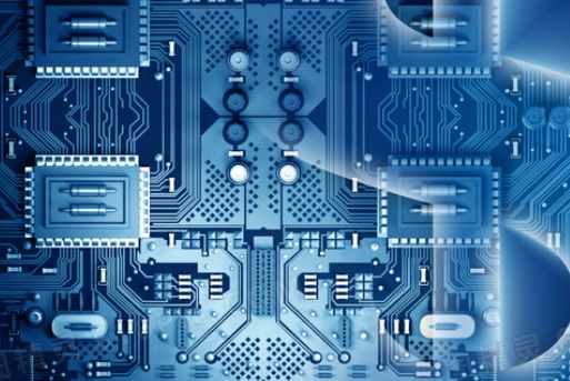
IPD technology, according to the process technology can be divided into thick film process and film process, Among them, the thick film process technology includes Low Temperature co-fired ceramics LTCC(Low temperature Co-firedCeramics) technology using ceramics as a substrate and PCB Embedded Passives technology based on HDI high density interconnection. The thin-film IPD technology uses commonly used semiconductor technology to make lines and capacitors, resistors and inductors.
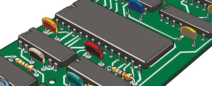
LTCC technology uses ceramic materials as a substrate, burying passive components such as capacitors and resistors into the ceramic substrate, and forming integrated ceramic components through sintering, which can greatly reduce the space of components. However, with the increase of the number of layers, the production difficulty and cost are higher, so LTCC components are mostly for a specific function of the circuit. PCB technology of HDI embedded components is usually used in digital systems, in this system is only suitable for distributed welding capacitors and low and medium precision resistors, with the reduction of component volume, SMT equipment is not easy to handle too small components. Although the embedded printed circuit board technology is the most mature, the product characteristics are poor, and the tolerance can not be accurately understood, because the components are buried in the multi-layer board, and it is difficult to replace or repair the adjustment after the problem. Compared with LTCC technology and PCB embedded component technology, the thin-film IPD technology of integrated circuits has the advantages of high precision, high repeatability, small size, high reliability and low cost, and is bound to become the mainstream of IPD in the future. This paper will mainly introduce the thin-film IPD technology.
3. Development status of thin-film integrated passive component technology
Thin film IPD technology uses exposure, development, coating, diffusion, etching and other thin film production processes. A representative profile diagram of the thin film integrated passive process is shown in Figure 1. This process can produce various resistors. Capacitors and inductors, as well as low-inductance ground floors and transmission line routes connecting passive components. The film structure is manufactured on the appropriate carrier substrate material, and the process must meet the required component performance and accuracy indicators, but also can not be complicated, and the mask number is less (generally 6 to 10 sheets). Each passive component typically occupies an area of less than 1mm2 in order to be able to compete with the discrete components of surface mount technology in terms of area and cost.


Just upload Gerber files, BOM files and design files, and the KINGFORD team will provide a complete quotation within 24h.