
Professional PCB manufacturing and assembly
Building 6, Zone 3, Yuekang Road,Bao'an District, Shenzhen, China
+86-13410863085Mon.-Sat.08:00-20:00

15 PCB Layout details
Printed Circuit Board (PCB) is a kind of electronic parts, it is the connection of electronic devices, such as ics, resistors, capacitors and inductors, etc. In PCB design, Layout design is crucial to the quality and performance of the final product. In this article, we will discuss 15 key details of PCB design to ensure that your PCB is safe from any potential problems and failures.
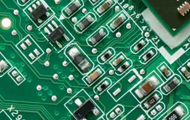
1. Component placement
The way components are arranged on the PCB board affects circuit performance and circuit density. In terms of component placement, wiring length, circuit number, and circuit noise must first be considered. Excessive accumulation or scattered placement should be avoided during placement.
Second, circuit board size
The size of the PCB has an impact on the performance and cost of the circuit. Under normal circumstances, the size of the PCB should be as small as possible in order to save space and materials as much as possible, reduce costs and improve performance efficiency. Third, PCB hierarchy
The hierarchy and number of one -, two -, and multi-layer PCBS and PCBS all have an impact on wiring, performance, and cost. Multilayer PCBS can greatly improve the wiring density and performance. When building multi-layer PCBS, the drawer effect must be avoided to ensure good performance of electrical signal transmission. Four, plate thickness
Board thickness has an important impact on PCB stiffness, stability and reliability. In PCB design, the thickness of the board should be controlled and ensure compliance with relevant regulations and standards. PCB routing rules are an important aspect of PCB design, and reasonable and accurate routing rules should be formulated and ensured. In the process of rule-making, signal integrity should be considered first, and other factors should be considered as far as possible. In PCB design, the circuit layout and sequence should be carefully planned to avoid circuit noise and interference.
Seven, PCB thermal management") https://www.kingfordpcb.com/yuan.php?time=1686665727
https://www.kingfordpcb.com/yuan.php?time=1686665727
The heat source has a great impact on the performance and reliability of the PCB. In the layout design, it is necessary to avoid the thermal effects of excessive density and higher power components on the PCB.
8. Types and specifications of PCB components
The type of PCB component has a great impact on the performance and cost of the circuit. Therefore, in PCB design, priority should be given to high-quality components that meet the specifications and requirements of the circuit. Nine, PCB board color and coating
The color and coating of the PCB board have an impact on the cost, reliability and performance of the PCB. When selecting colors and coatings, their use scenarios and standard regulations should be considered.
Ten, PCB board may appear problems
Poor etching, poor in-layer hole contact and areas that have not passed the test can all lead to failures of PCB hardware and circuits. In the PCB production and manufacturing process, we should pay close attention to these problems and take relevant measures to solve them.
In PCB manufacturing, the quality of drilling has a direct impact on deviation and error. The number, size and location of holes should be strictly controlled during the design and manufacturing process to ensure accuracy.
Local strengthening of PCB to improve the quality and stability of PCB board, local strengthening is necessary. The strengthening method should be determined according to the layout design requirements and use scenarios of the PCB board.
13. High-speed transmission signal broadcasting
High-speed signal transmission is one of the key issues in PCB design, and appropriate design and measures need to be taken to safeguard its signal integrity and circuit performance.
14. Total cost of PCB
In the PCB manufacturing and design phase, the total cost of the PCB should always be focused on and cost reduction. Using less material and less space, and using more economical PCB processing processes and technologies are key to achieving a lower total cost.
15, PCB standards and regulations In the PCB design and manufacturing process, should always comply with the relevant standards and regulations and ensure that PCB quality meets the requirements and standards.
PCB board wiring for high resolution ADC
Jun 13,2023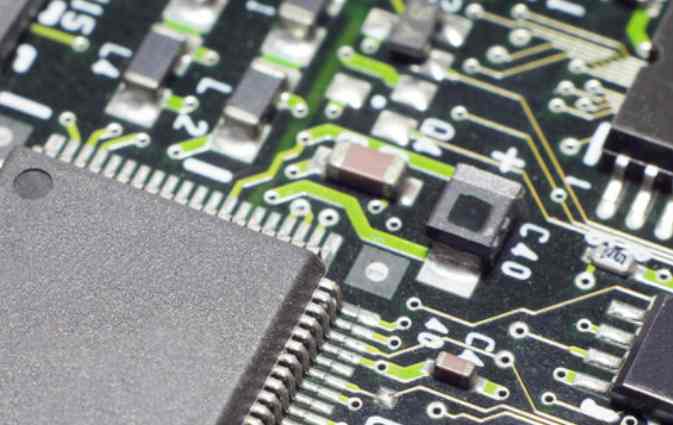


Just upload Gerber files, BOM files and design files, and the KINGFORD team will provide a complete quotation within 24h.