
Professional PCB manufacturing and assembly
Building 6, Zone 3, Yuekang Road,Bao'an District, Shenzhen, China
+86-13410863085Mon.-Sat.08:00-20:00

Functional testing is becoming increasingly important, however, as with online testing, technological developments and PCB designs can limit the scope of testing. While great progress has been made in programming software environments that can help overcome some of these difficulties, there are many more problems to avoid and better prepare for if you want to successfully implement functional testing in accordance with your testing strategy. This paper introduces some factors that should be considered in the successful implementation of functional testing and countermeasures.

Functional testing of electronic products has a history of ups and downs. In the late 1960s, it was the first automated testing method. With the emergence of online testing technology in the late 1970s, functional testing seemed destined to give way to online testing that became easier and faster to program and judge. Now, however, the tide has turned again. Online testing has a problem that is getting more and more serious, that is, the detection method. According to the United States NEMI(National Electronics Manufacturing Organization) analysis, by the end of 2003, the number of detectable nodes will be basically zero, if it can not be detected, then online testing is almost useless.
Functional testing is increasingly used in post-production processes and even mid-process testing, but its system and implementation methods are almost completely different from previous testing. Today's test systems are faster and more compact in most cases, and functional testing is essential for verifying the overall functionality of products, maintaining calibration information, providing data to ISO9000 procedures, and assuring the quality of high-risk products such as medical devices.
How testing is performed is influenced by factors such as budget, yield, and the design of the product under test (UUT), and it is the last item that has the greatest impact on what can be measured, with budget and yield limiting what is tested. In order to make the test as high as possible failure coverage, in the design stage must pay attention to the selection of components and PCB layout, unfortunately, the actual situation is not always the case, rush to market and nervous development often disrupt your wishful thinking.
Here is a preliminary analysis of how to deal with these constraints. Some compromises that have to be made to test, especially in the early design stages, may affect the design, but make testing easier and improve test failure coverage. Please note that the following issues and recommendations are not something that every test engineer will face or need to address, and many of these issues will affect each other, so each should be evaluated and flexibly applied as needed.
What are the test requirements for the product under test?
Before discussing design, test systems, software, and test methods, it is important to understand the "object" - the product to be tested, not only the PCB or final assembly itself, but also how much will be produced, expected failures, and so on, including:
Product category
Structure (Single PCB/ pre-made PCB/ final product)
Test specification
Planned test point
Expected production (per line/day/shift, etc.)
Expected failure type
Obviously, the "budget" is ignored above, but only when you understand the above can you determine how much a product will cost to test, only when you know what it will take to fully test the UUT can you start talking about funding, and only then can you know how to compromise to get the job done. After the initial presentation is completed, the company may give you a budget and wish you "good luck" - figure out what you can do, and "good luck" is needed, but there are other things, some of which are listed below.
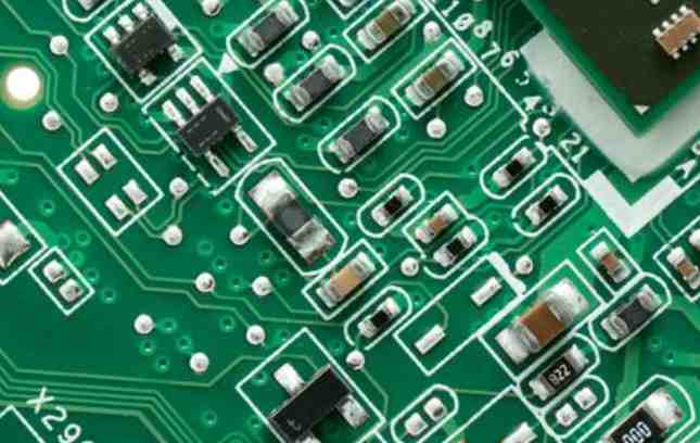
High density problem
On the surface, component density does not seem to be a problem for functional testing, after all, the main concern here is "getting the right output for an input". Admittedly, it is a little simplistic, but that is the reality. When a given excitation signal is applied to the input end of the UUT, the UUT will output a specific series of data after a certain time, and the connection with the I/O connector should be the only access problem.
But component density also has a certain impact, look at the PCB sample in Figure 1 (or your own design), you first have to answer the following questions;
Do I need to plug in the calibration circuit?
Is it important to diagnose specific UUT components or specific areas?
If the answer to these questions is yes, is the probe done by a human or by some kind of automatic device?
Do you want to use automated test equipment?
Is the I/O connector used easy to reach or connect? If not, is the connector a through-hole mounting that can be reached through the needle bed?
15 PCB Layout details
Jun 13,2023


Just upload Gerber files, BOM files and design files, and the KINGFORD team will provide a complete quotation within 24h.