
Professional PCB manufacturing and assembly
Building 6, Zone 3, Yuekang Road,Bao'an District, Shenzhen, China
+86-13410863085Mon.-Sat.08:00-20:00

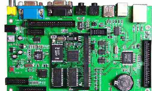
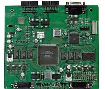
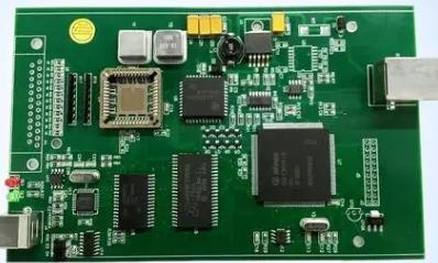
Professional pcba proofing manufacturers printed circuit board (PCB) sample collection
This article "Professional pcba proofing manufacturers printed circuit board (PCB) sample collection" is kinhford Electronic Technology Co., LTD. PCBA author edited, welcome to read the following details.
1) Cots installation quality assessment industry: display, printed circuit board, lead frame, etc
Challenge: Laminating defects can occur if the rubber has poor adhesion to the steel core of the laminating roll, or if the rubber is damaged. Benefits of Prescale: Saves time, improves quality
2) Measurement of scraper pressure distribution in the solder paste printing process industry: printed circuit board (PCB) electronic component installation challenge: When printing paste solder screen onto the printed substrate, any non-uniformity of scraper pressure distribution will result in uneven application of paste solder. Benefits of Prescale: Saves time, saves materials, improves quality
(3) Check the adhesive pressure of dry film resist (DFR) lamination") https://www.kingfordpcb.com/yuan.php
https://www.kingfordpcb.com/yuan.php
Industry: Printed circuit Board (PCB), lead frame, LCD, etc
Challenge: Bubbles and wrinkle uniforms can form if the base material/dry film resist/laminate roll is not balanced or the pressure is not properly adjusted. Benefits of Prescale: Save time, save materials
(4) Check mold contact and pressure uniformity of laminates or laminates. Industries: laminates ceramics, ceramic substrates and packages, PCBS, automotive and mobile phone electronic components, laminates equipment manufacturing
Challenge: Pressing with extremely high precision is required to avoid changes in electrical characteristics due to problems with poor adhesion or uneven thickness, and to avoid electrical connection failures due to shifting electrode patterns. Benefits of Prescale: Increased production, improved quality, and improved accuracy
5) Pressure Uniformity Verification of vacuum hot pressing devices Industries: Electronic components, OLeds, touch screens, printed circuit boards, semiconductor equipment used to manufacture and develop machines and other challenges: Expect or require equipment to maintain as even a surface pressure as possible to improve the quality of processed products.
Impedance matching means that when transmitting the source, the load impedance must equal the characteristic impedance of the transmission line. In this case, the transmission will not reflect, indicating that all sources have been absorbed by the load. Instead, there is a source loss during transmission. In HDI PCB design, impedance matching is related to signal quality.
When does PCB routing require impedance matching?
It is not primarily determined by frequency, but the key is the steepness of the signal, i.e. the time the signal goes up/down. It is generally considered that if the signal's rise/fall time (based on 10% to 90%) is less than 6 times the line delay, it is a high speed signal and attention must be paid to impedance matching. Wire delay is usually set to 150ps/inch.
Characteristic impedance
During the transmission of the signal along the transmission line, if there is a consistent signal propagation speed everywhere along the transmission line and the capacitance per unit length is the same, the signal will always see a perfectly consistent instantaneous impedance as it travels. Since the impedance remains constant throughout the transmission line, we use a specific name for the characteristic or the characteristic of a particular transmission line, which is called the characteristic impedance of a transmission line. Characteristic impedance is the instantaneous impedance value when the signal is seen along the transmission line. The characteristic impedance is dependent on the board where the PCB leads are located, the material (dielectric constant) used by the PCB, the width of the wire, and the distance between the conductor and the pad, independent of the length of the wire. Software can be used to calculate the characteristic impedance. In HDI PCB designs, the linear impedance of the digital signal is usually designed to be 50 ohm, which is an approximation. Typically, coaxial cable has a 50 ohm base band, 75 ohm frequency band, and 100 ohm for twisted pair (differential).


Just upload Gerber files, BOM files and design files, and the KINGFORD team will provide a complete quotation within 24h.