
Professional PCB manufacturing and assembly
Building 6, Zone 3, Yuekang Road,Bao'an District, Shenzhen, China
+86-13410863085Mon.-Sat.08:00-20:00

Printed circuit board(PCB) is an important part of modern electronic equipment, but also an important carrier of electronic components and electrical connections. China has a large global demand for consumer electronic products, and PCB market has maintained a growing trend. However, the industry started late, lacks technical reserves, and the generation gap between industrial products and the international mainstream. In high-end circuit, a large number of core components board and board rely on imports, and the situation is extremely severe. In terms of stimulus factors, the Chinese people began to self-road PCB copy board counterattack, Xiaobian believes that innovation can really be realized, but also lies in the improvement of the technical level, patent reserves and product evolution of the layout of research and development.

Industry status: PCB copy board in urgent need of integration and reorganization
People may still stay in the past "imitation" and "imitation" concept, PCB copy board how can lead us to self-reliance? Just as the history is constantly evolving, PCB board industry is also constantly changing. After the impact of the global economic downturn in 2013, PCB board industry has been faced with many problems, mainly manifested in the following aspects: one is the single copy enterprise and product type, lack of development of electric power; Second, relative excess capacity, industry integration is imminent; Three industries manage medium - body industry, support misunderstanding, lack of development. In this regard, China's PCB copying board industry has been constantly transforming and upgrading, strengthening technological innovation and industry integration and restructuring.
Copying board technology: digestion and innovation on a high starting point
In the past, maybe PCB copying board was just copying PCB file, making BOM list and backdrawing schematic according to the mother board or prototype provided by the customer, and then completing the process of welding, debugging and making the prototype. However, PCB copy board is now more of a process of learning digestion and absorption. This innovative way of R&D at a high starting point can not only avoid industry risks, reduce the R&D cycle, but also greatly improve the cost performance ratio, which is of great benefit to the cost, financial pressure and international competitiveness of our PCB enterprises at the present stage.
Looking to the future, PCB copying board industry is still optimistic about the mobile Internet, three networks integration, cloud computing, smart grid, new energy vehicles as a representative of the rapid development of strategic emerging industries, will become the future computer, network communication, consumer electronics products, to promote the development of PCB copying board new power. Guangzhou SMT small series, with the continuous development of society, automation, intelligent, hardware facilities of the direction of intelligent PCB board changes has become a top priority. In the tide of domestic smart city construction, strengthening the localization of PCB copy board will strongly support the wisdom of the development of all walks of life.
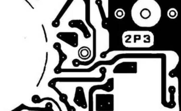
How much distance must be left between the parts and the board edge during PCB design
In PCB design, how much distance must be left between the parts and the edge of the board so as not to affect the electrical properties? (If the material is FR4, there are SMT parts on both sides, there are board design, and there are two processing methods of Routing and V-CUT between boards)
Is it possible to control the Tolerance of the finished product aperture more effectively if the Annular ring width of the fortifying mouth is used? This problem has a lot to do with SMT equipment. Most equipment requires at least 0.150 inch retaining edge as a safe distance for assembling and conveying splints. If Panel design is used, the break treatment between pieces can be designed with V-c ut or stamp holes.
The V-cut path is reserved for 20? 30mil width with no conductor residue on it (calculated from the V-ciit center line to the sides) is ideal. However, some manufacturers in order to prevent stay, deliberately design a line on the V-cut path, in the electrical measurement can be used as a missing cut indicator.
It is true that increasing the Annular ring width can effectively control the finished product aperture tolerance concept. We can understand it from the following aspects: (1) If the Pad can be increased in the high current region or independent hole in the circuit board electroplating process, its average current density can be reduced, which naturally reduces the difference between the copper thickness of the hole in this region and other areas.
(2)Annular ring is large, and the Solder residue in the hole can also be reduced in the solder spraying process. If other electroplated metal surface treatment is used, the current density can be homogenized and the aperture difference can be reduced. The above is for your reference.
Chemical deburring process of PCB circuit board
Jun 01,2023


Just upload Gerber files, BOM files and design files, and the KINGFORD team will provide a complete quotation within 24h.