
Professional PCB manufacturing and assembly
Building 6, Zone 3, Yuekang Road,Bao'an District, Shenzhen, China
+86-13410863085Mon.-Sat.08:00-20:00

Which PCB design company is good? There are so many companies that can do PCB design in Shenzhen, which one is good? The main thing is to compare the cost and delivery time. Shenzhen kingford is a professional PCB design company with an average PCB design team with more than years of working experience. We can skillfully use the mainstream PCB design software in the market and communicate professionally and efficiently to ensure the progress of PCB design, so as to help you seize the market opportunity earlier!
What is PCB design?
PCB design is based on the circuit schematic diagram to achieve the function required by the circuit designer. PCB design mainly refers to layout design, which needs to consider the layout of external connections. Optimized layout of internal electronic components. Optimized layout of metal wires and through holes. Electromagnetic protection. Heat dissipation and other factors. Excellent layout design can save production cost, achieve good circuit performance and heat dissipation performance. Simple layout design can be realized by hand, complex layout design needs to be realized by computer aided design (CAD).
PCB design advantage
Shenzhen Honglijie own PCB board factory, SMT plant, familiar with various production parameters. The PCB design process is rigorous and standardized, in line with the process requirements of mainstream PCB board factories and assembly manufacturers. PCB design parameters are not only suitable for the research and development phase, but also fully consider the mass production characteristics. We insist on one time to do things well, reduce the number of research and development, reduce the cost of research and development, so that your products quickly to the market, seize the opportunity.
PCB design capability
Shenzhen kingford has the capability of PCB design with the following parameters:
Maximum signal design rate: 10Gbps CML differential signal;
Maximum number of PCB design layers: 40;
Minimum line width: 2.4mil;
Minimum line spacing: 2.4mil;
Minimum BGA PIN spacing: 0.4mm;
Minimum mechanical hole diameter: 6mil;
Minimum laser drilling diameter: 4mil;
Maximum number of pins:; 63000 +
Maximum number of components: 3600;
Maximum number of BGA: 48+.
PCB design covers the product
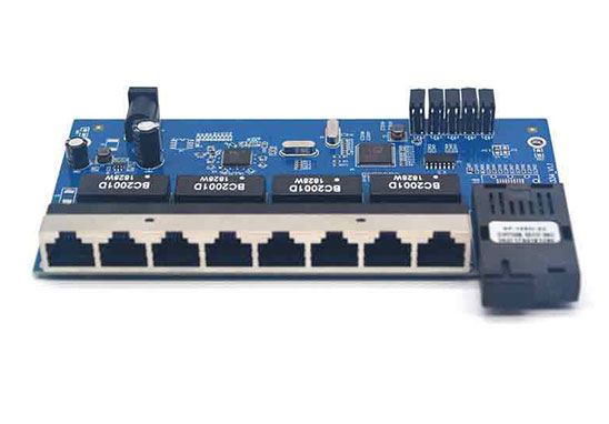
1. PCB design of IT communication products
Switch, router, VOIP, xDSL, 3G/4G /5G office/terminal equipment of all types, backbone and access network transmission equipment, optical network, network transmission storage equipment, mass storage, etc.
2. PCB design of multimedia products
Video telephone, conference TV, LCD TV/monitor, monitoring and security equipment, burning equipment, etc.
3. PCB design of computer products
Servers, laptops, network storage, tablets, ultrabooks, cloud computing, etc.
4. PCB design of industrial control products
Artificial intelligence, machine vision, intelligent manufacturing equipment, smart power grid, distribution network equipment, clean energy equipment, construction machinery, agricultural machinery, fire equipment and other industrial automation equipment.

5. PCB design of aerospace products
Flight control system, micromotor system, navigation system, satellite, communication system, airborne audio-visual entertainment equipment, airborne communication equipment, unmanned aerial vehicle, etc.
6. PCB design of medical device products
Ultrasonic, nuclear magnetic resonance equipment, CT, IVD in vitro diagnosis, infrared temperature measurement, blood coagulation detection, nucleic acid analyzer, digital X-ray imaging, dry chemical analyzer, chemiluminescence instrument and other detection, analysis, monitoring equipment.
7. PCB design of rail transit products
New energy vehicles, autonomous driving system, automobile intelligent network management system, rail transit vehicles and all kinds of mechanical and electrical equipment, rail transit autonomous operation system, train dispatching command system, detection equipment, etc.
8. PCB design of digital electronic products
Smart phones, PDAs, digital cameras, e-books, GPS, wearable devices, VR, Internet of smart Things, etc.
PCB design service process
1. Data provided by the customer: schematic diagram, network table, structure diagram, device data to be built, design requirements, etc.;
2. Layout and wiring review: CHECKLIST shall be conducted according to Macrolite design specifications, design instructions, customer design requirements and related checklist;
3. Customer layout confirmation: kingford provides layout documents and structure documents for customers to conduct layout review; Customer confirms layout rationality, cascade scheme, impedance scheme, structure, packaging, and confirm wiring parameters;
4. Design data output: PCB source files, Gerber files, assembly files, steel mesh files, structure files, etc.


Just upload Gerber files, BOM files and design files, and the KINGFORD team will provide a complete quotation within 24h.