
Professional PCB manufacturing and assembly
Building 6, Zone 3, Yuekang Road,Bao'an District, Shenzhen, China
+86-13410863085Mon.-Sat.08:00-20:00


As the carrier of various components and the hub of circuit signal transmission, PCB board has become the most important and key part of electronic information products, its quality and reliability level determines the quality and reliability of the whole equipment. However, due to the reasons of cost and technology, there are a lot of failure problems in the process of PCB production and application.
So there are some common failure analysis techniques that are used. In view of the structural characteristics of PCB and the main failure modes, this paper will focus on nine techniques for PCB failure analysis, including: appearance inspection, X-ray fluoroscopy, metallographic section analysis, thermal analysis, photoelectron spectroscopy analysis, microscopic infrared analysis, scanning electron microscopy analysis and X-ray spectroscopy analysis. Metallographic slice analysis is one of the destructive analysis techniques. Once these two techniques are used, the sample will be destroyed and cannot be recovered. In addition, due to the requirements of sample preparation, SEM analysis and X-ray energy spectrum analysis may sometimes require partial destruction of the sample. In addition, in the process of analysis, due to the need of failure location and verification of failure causes, it may be necessary to use test techniques such as thermal stress, electrical properties, weldability testing and dimensional measurement, which will not be specifically introduced here.
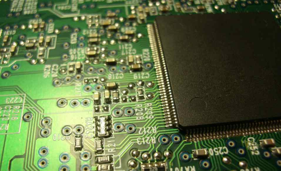
1. Appearance inspection Appearance inspection is to visually inspect or use some simple instruments, such as stereoscopic microscope, metallographic microscope and even magnifying glass, to check the appearance of the circuit board and find the failure site and related material evidence. The main function is to locate the failure and preliminarily judge the failure mode of PCB. Appearance inspection mainly checks PCB contamination, corrosion, the location of burst board, circuit wiring and the regularity of failure, such as batch or individual, is always concentrated in a certain area and so on. In addition, many PCB failures are discovered after assembly into PCBA. Whether the failure is caused by the influence of the assembly process and materials used in the process also requires careful inspection of the characteristics of the failure area.
2. X-ray fluoroscopy inspection For some parts that cannot be inspected by appearance, as well as PCB through hole interior and other internal defects, X-ray fluoroscopy system has to be used for inspection. X-ray perspective system is the use of different material thickness or different material density to X-ray moisture absorption or permeability of different principles to image. This technique is more commonly used to check for defects inside PCBA solder joints, through hole internal defects, and defect spot positioning in high-density packaged BGA or CSP devices. At present, the resolution of industrial X-ray equipment can reach less than one micron, and is changing from two-dimensional to three-dimensional imaging equipment, and even five-dimensional (5D) equipment has been used for packaging inspection, but this 5D X-ray system is very valuable, rarely has practical application in the industry.
3. Slice analysis Slice analysis is the process of obtaining the cross-section structure of PCB circuit board through a series of means and steps such as sampling, Mosaic, slice, polishing, corrosion and observation. Through slice analysis, we can get rich information about the microstructure of PCB (through hole, coating, etc.) quality, which provides a good basis for the next step of quality improvement. But this method is destructive, once the slice is made, the sample is bound to be destroyed; At the same time, this method has high requirements and time-consuming sample preparation, which requires trained technicians to complete.
Why does the PCB board have to be impedance?
Mar 04,2023


Just upload Gerber files, BOM files and design files, and the KINGFORD team will provide a complete quotation within 24h.