
Professional PCB manufacturing and assembly
Building 6, Zone 3, Yuekang Road,Bao'an District, Shenzhen, China
+86-13410863085Mon.-Sat.08:00-20:00

The quality of package will directly affect the performance of chip itself and PCB design and manufacture connected with it. Therefore, packaging technology is crucial.
An important indicator to measure whether a chip packaging technology is advanced or not is the ratio of chip area to package area. The closer the ratio is to 1, the better.
The main factors to consider when packaging:
The ratio of chip area to package area should be as close to 1:1 as possible in order to improve packaging efficiency;
Pins should be as short as possible to reduce delay, and the distance between pins should be as far as possible to ensure non-interference and improve performance;
Based on heat dissipation requirements, the thinner the package, the better.
Packaging has roughly evolved through the following processes:
Structure: TO→DIP→PLCC→QFP→BGA→CSP
Materials: Metal, ceramic → ceramic, plastic → plastic
Pin shape: long lead straight, short lead or no lead attachment, ball convex point
Assembly mode: through hole insertion → surface assembly → direct installation
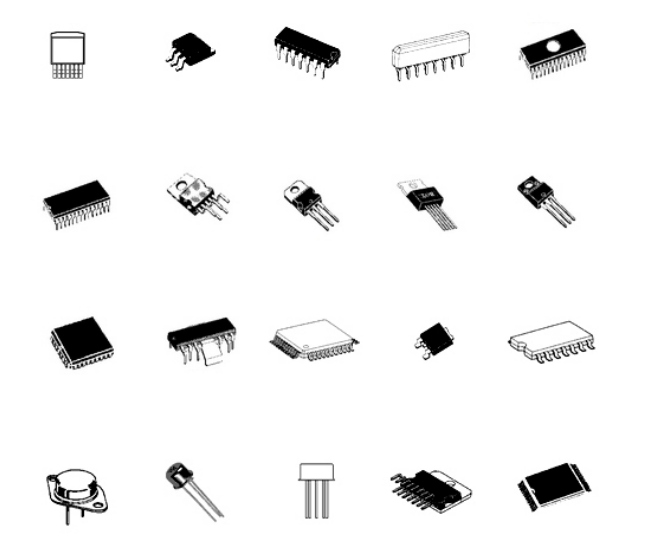
The following is the specific packaging form:
1. SOP/SOIC encapsulation
SOP stands for Small Outline Package.
SOP packaging technology was developed by Philips in 1968 ~ 1969 and subsequently evolved into:
lSOJ, J-pin small shape package
lTSOP, thin and small shape package
lVSOP, very small shape package
lSSOP, reduced SOP
lTSSOP, thin reduced SOP
lSOT, small profile transistor
lSOIC, small shape integrated circuit
2. DIP encapsulation
DIP is the abbreviation of the English "Double In-line Package", that is, double in-line package.
One of the plug-in package, the pin from both sides of the package, packaging materials are plastic and ceramic two kinds. DIP is the most popular plug-in package, the application range includes standard logic IC, memory LSI, microcomputer circuits, etc.
3, PLCC packaging
PLCC is the abbreviation of the English "Plastic Leaded Chip Carrier", namely, plastic J lead chip package.
PLCC package, shape is square, 32 pin package, pin around, shape size is much smaller than DIP package. PLCC package is suitable for mounting wiring on PCB with SMT surface mounting technology, which has the advantages of small size and high reliability.
4. TQFP encapsulation
TQFP is the abbreviation of the English "Thin Quad Flat Package", namely, thin plastic encapsulation four corner flat package. The four-sided flat packaging technology can effectively use space, thus reducing the size of the printed circuit board.
Due to the reduced height and volume, this packaging process is well suited for applications with high space requirements, such as PCMCIA cards and networking devices. Almost all ALTERA CPLDS/FPGas have TQFP packaging.
5. PQFP encapsulation
PQFP is the abbreviation of "Plastic Quad Flat Package".
PQFP package chip pin distance is small, pin is very thin. General large-scale or very large scale integrated circuits adopt this form of packaging, its pin number is generally more than 100.
6. TSOP encapsulation
TSOP is the abbreviation of "Thin Small Outline Package", that is, thin and small size package. A typical feature of TSOP memory packaging technology is to make pins around the packaging chip. TSOP is suitable for mounting wiring on PCB board using SMT (surface mount) technology.
TSOP package shape, reduced parasitic parameters (current changes greatly, the output voltage disturbance), suitable for high frequency applications, easy to operate, and high reliability.

7. BGA encapsulation
BGA is the abbreviation of "Ball Grid Array Package", namely, ball grid array package. In the 1990s, with the progress of technology, chip integration continues to improve, the number of I/O pins increases sharply, power consumption also increases, and the requirements for integrated circuit packaging are more stringent. In order to meet the needs of development, BGA packaging began to be used in production.
The memory encapsulated by BGA technology can increase the memory capacity by two to three times without changing the memory volume. Compared with TSOP, BGA has smaller volume, better heat dissipation and electrical performance. BGA packaging technology has greatly increased the amount of storage per square inch. Memory products using BGA packaging technology are only one-third of the volume of TSOP packaging for the same capacity. In addition, compared with traditional TSOP packaging, BGA packaging has a faster and more effective way to dissipate heat.
The I/O terminals of BGA package are distributed under the package in the form of array with circular or cylindrical solder joints. The advantage of BGA technology is that although the number of I/O pins increases, the spacing of pins increases instead of decreasing, thus improving the assembly yield. Although its power consumption is increased, BGA can be welded by controlled collapse chip method, which can improve its electric heating performance. Thickness and weight are reduced compared to previous packaging techniques; The parasitic parameter is reduced, the signal transmission delay is small, and the use frequency is greatly increased. Assembly can be coplanar welding, high reliability.
8, TinyBGA packaging
When it comes to BGA packaging, it is necessary to mention Kingmax's patented TinyBGA technology. TinyBGA English full name "Tiny Ball Grid", belongs to a branch of BGA packaging technology, is Kingmax company in August 1998 developed successfully. The ratio of chip area to package area is no less than 1:1.14, which can improve the memory capacity by 2 ~ 3 times with the same memory volume. Compared with TSOP packaged products, it has a smaller volume, better heat dissipation performance and electrical performance.
Memory products using TinyBGA packaging technology, under the same capacity condition, only 1/3 of the volume of TSOP packaging. TSOP encapsulated memory pins are led from around the chip, while TinyBGA is led from the center of the chip. In this way, the transmission distance of the signal is effectively shortened. The length of the signal line is only 1/4 of that of the traditional TSOP technology, so the signal attenuation is reduced. This not only greatly improves the anti-interference, anti-noise performance of the chip, but also improves the electrical performance. The TinyBGA package can resist up to 300MHz external frequency, while the traditional TSOP package technology can resist up to 150MHz external frequency.
TinyBGA memory is thinner (package height less than 0.8mm), and the effective heat dissipation path from the metal substrate to the heat dissipation body is only 0.36mm. As a result, TinyBGA memory has higher heat transfer efficiency and is ideal for long running systems with excellent stability.
9. QFP encapsulation
QFP stands for "Quad Flat Package", a flat package of small blocks. QFP package was used more frequently in early graphics cards, but few QFP package video memory speed above 4ns, because of the process and performance problems, has been gradually replaced by TSOP-II and BGA. QFP encapsulation around the particle with pins, recognition is quite obvious. Four-side pin flat package. One of the surface mount type packages, with the pins leading from the four sides in a seagull wing (L) shape.
There are three substrates: ceramic, metal and plastic. In terms of number, plastic packaging accounts for the vast majority. When no material is specified, plastic QFP is used in most cases. Plastic QFP is the most popular multi-pin LSI package, not only used in microprocessor, door display and other digital logic LSI circuits, but also used in VTR signal processing, audio signal processing and other analog LSI circuits.
Pin center distance has a variety of specifications, such as 1.0mm, 0.8mm, 0.65mm, 0.5mm, 0.4mm, 0.3mm, 0.65mm center distance specification, the maximum number of pins in the 0.65mm center distance specification is 304.


Just upload Gerber files, BOM files and design files, and the KINGFORD team will provide a complete quotation within 24h.