
Professional PCB manufacturing and assembly
Building 6, Zone 3, Yuekang Road,Bao'an District, Shenzhen, China
+86-13410863085Mon.-Sat.08:00-20:00

I. Composition:
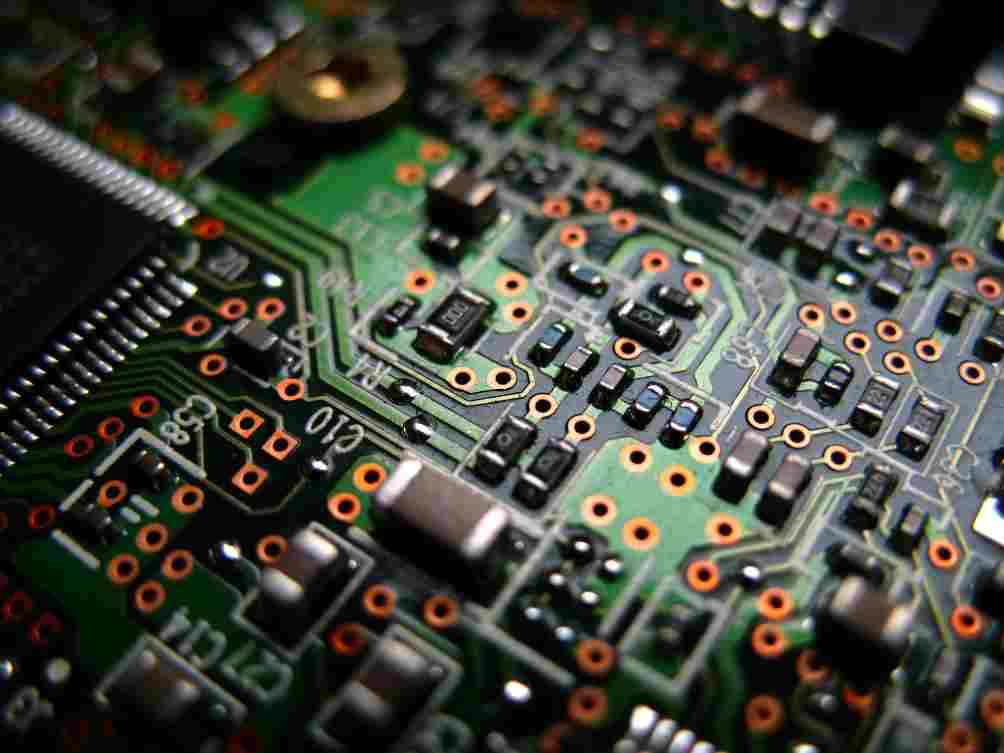
The circuit board is mainly composed of welding pad, through hole, mounting hole, wire, components, connectors, filling, electrical boundary, etc. The main functions of each component are as follows:
1. Welding pad: metal hole for welding pin of components.
2. Through hole: there are metal through holes and non-metal through holes, among which metal through holes are used to connect the pins of components between each layer.
3, mounting hole: used to fix the circuit board.
4. Conductor: electrical network copper film for connecting component pins.
5. Connectors: components used for connecting circuit boards.
6, filling: used for ground wire network of copper, can effectively reduce the impedance.
7, electrical boundary: used to determine the size of the circuit board, all the components on the circuit board can not exceed the boundary.
Two, the main classification
Circuit board systems are classified into the following three types:
1. Single panel
We call printed circuit board single panel. Only early circuits used such boards because single panels had many severe limitations on the design circuit (because they had only one side, the wires could not cross and had to go around a separate path).
2. Double panel
The circuit board has wiring on both sides. But to use both wires, there must be a proper circuit connection between the two sides. This "bridge" between circuits is called a pilot hole (via). A pilot hole is a small hole in a PCB filled with or coated with metal that can be connected to wires on both sides. Because the area of a dual panel is twice as large as that of a single panel, and because the wiring can be interleaved (it can go around to the other side), it is better suited for more complex circuits than a single panel.
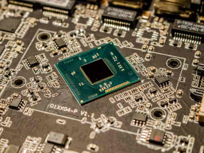
3. Multi-layer board
Multilayer board in the more complex application needs, the circuit can be arranged into a multi-layer structure and pressed together, and in the layer lay a through hole circuit to connect the circuit of each layer.
Inner circuit
Copper foil substrate is first cut to size suitable for processing production. Before pressing the substrate film, it is usually necessary to coarse the copper foil on the surface of the substrate properly by brush grinding, micro-etching and other methods, and then attach the dry film photoresist tightly to it at the appropriate temperature and pressure. The substrate pasted with dry film photoresist is sent to the UV exposure machine for exposure. The photoresist will produce polymerization reaction after ultraviolet irradiation in the film transmittance area (the dry film in this area will be retained as etching resistance in the later development and copper etching steps), and the line image on the negative will be transferred to the dry film photoresist on the surface of the plate. After tearing off the protective adhesive film on the film surface, the development of the unilluminated area on the film surface is removed with sodium carbonate aqueous solution, and then the exposed copper foil is corroded and removed with hydrochloric acid and hydrogen peroxide mixed solution to form a circuit. Finally, the successful dry film was photoresist washed with sodium hydroxide aqueous solution. For the inner circuit board of six or more layers, the automatic positioning punching machine is used to flush out the rivet reference hole of interlayer line alignment.
pressing
In order to increase the area that can be wired, more single or double sided wiring boards are used in multilayer boards. Multilayer plates are made of several double panels, and a layer of insulation is placed between each layer of plates and glued firmly (pressed together). The number of layers on the board means that there are several separate wiring layers, usually with an even number of layers, including the two outermost layers. Most main board is 4 to 8 layer structure, but technically can do dozens of layers of PCB board. Most large supercomputers use quite a few layers of mainframe boards, but because such machines can be replaced by clusters of ordinary computers, super-multiboards have fallen out of use. Because the layers in a PCB are so tightly integrated, it is not always easy to see the actual number, but if you look closely at the host board, you may be able to see it.
How to reduce SMT patch processing pollution
Feb 08,2023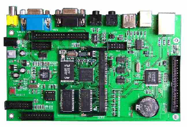


Just upload Gerber files, BOM files and design files, and the KINGFORD team will provide a complete quotation within 24h.