
Professional PCB manufacturing and assembly
Building 6, Zone 3, Yuekang Road,Bao'an District, Shenzhen, China
+86-13410863085Mon.-Sat.08:00-20:00

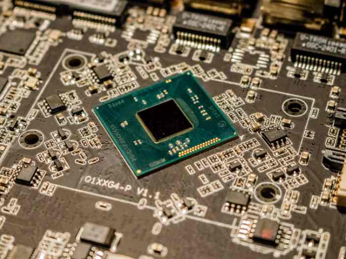
In recent years, the focus of the printed circuit board market has shifted from computers to communications, and in the past two years it has shifted to mobile terminals such as smart phones and tablet computers. Therefore, mobile terminal with HDI board is the main point of PCB growth. The mobile terminal represented by smart phone drives HDI board higher density and thinner. PCB all to high density fine line development, HDI board is particularly prominent.
Semi-addition substrate
Now the hot spot of semi-addition method is the use of insulating dielectric film layer, from the fine line realization and production cost, SAP is more favorable than MSAP. SAP deposition with heat curing resin, by laser drilling after electroplating copper to form a through hole and circuit pattern. At present, the HDI lamination materials in the world use epoxy resin with different curing agents to add inorganic powder to improve material rigidity and reduce CTE, and also use glass fiber cloth to enhance rigidity.
Copper plating and hole filling
For reliability, electroplated copper filling technology is adopted for interconnection holes, including blind hole filling and through hole filling. The ability of copper plating to fill holes is shown in the filling property: whether there is a void in the hole closed by copper; Flatness: the degree of Dimple in the copper plating orifice; Thickness to diameter ratio: the ratio of plate thickness (hole depth) to the aperture.
Inverted chip packaging IC seal loading plate technology
Organic substrates account for more than one-third of the global semiconductor packaging market. FC-CSP and FC-PBGA have surged as the production of mobile phones and tablets has grown. The organic substrate replaces the ceramic substrate. The pitch of the sealing plate is becoming smaller and smaller, with a typical line width/line pitch now of 15µm. Future development trend. Fine-spaced carrier plates will continue in BGA and CSP, while core-free plates and four or more layers of carrier plates will be used more. The road map shows that carrier plates feature smaller sizes and performance focuses on low dielectric properties, low thermal expansion coefficient and high heat resistance, and the pursuit of low-cost substrate on the basis of meeting performance objectives.
Adapt to high frequency and high speed requirements
Electronic communication technology from wired to wireless, from low frequency, low speed to high frequency, high speed. Now mobile phone performance has entered 4G and will move towards 5G, which means faster transmission speed and larger transmission capacity. With the advent of the global cloud computing era, the data flow has multiplied and the high frequency and high speed of communication equipment is an inevitable trend. PCB for high frequency, high speed transmission needs, in addition to circuit design to reduce signal interference and loss, maintain signal integrity, and PCB manufacturing to maintain in line with the design requirements, it is important to have a high performance substrate. To solve PCB increase speed and signal integrity, mainly for electrical signal loss properties.
Improve heat resistance and heat dissipation
With the miniaturization and high function of electronic equipment, high heating is generated, and the thermal management requirements of electronic equipment are increasing. One of the solutions chosen is the development of thermal conductive printed circuit boards. PCB is required to have high thermal conductivity and heat resistance, and has been working on this for nearly ten years. Existing high heat dissipation PCB such as flat thick copper base PCB, aluminum metal base PCB, aluminum metal core double-sided PCB, copper base flat PCB, aluminum base cavity PCB, embedded metal block PCB, flexible aluminum base PCB. The use of metal substrate (IMS) or metal core printed circuit board, to play the role of heat dissipation components, compared with the traditional radiator, fan cooling to reduce the size and cost. At present, most metal substrates or metal cores are metal aluminum.
New trend of flexible and rigid plate technology
The miniaturization and thinness of electronic equipment inevitably use flexible PCB and rigid flexible combined PCB (R-FPCB). With the expansion of applications, there will be many new performance requirements in addition to the increasing number of applications. Polyimide membrane has colorless transparent, white, black and yellow and other different types, with high heat resistance and low CTE properties, to suit different occasions. There is also a market for cost-effective mylar substrates, where new performance challenges include high elasticity, dimensional stability, film surface quality, as well as the film's photocoupling and environmental resistance to meet the changing requirements of end users. FPCB and rigid HDI board to adapt to high speed and high frequency signal transmission requirements, the dielectric constant and dielectric loss of flexible substrate must be paid attention to, using polytetrafluoroethylene and advanced polyimide substrate to form flexible circuit. By adding inorganic powder and carbon fiber filler to polyimide resin, a three-layer flexible thermal conductive substrate can be produced. Inorganic fillers are aluminum nitride (AlN), alumina (Al 2O3) and hexagonal boron nitride (HBN).
Printed electronics technology
Printed electronic history is very long, only in recent years the momentum. The continuous development of printed electronics can see the prospect of commercial application is very broad, now there are PCB manufacturers into printed electronics, they start from flexible board, with printed electronic circuit (PEC) instead of printed circuit board (PCB). Printed electronic technology is the closest to FPCB, the current substrate and ink materials are various, once the performance and cost breakthrough will be a large number of applications, reduce the cost will open up a larger market. Traditional hybrid systems that combine silicon and printed electronic components may open up a new PCB industry. In addition to the use of some polymer materials, printed electronics also need functional ink materials, mainly conductive ink, constantly to improve the conductivity, printing adaptability, low cost development, currently available for printed electronic products to choose conductive ink has a lot of types. There are also piezoelectric, thermoelectric and ferroelectric materials, which can be used together in printed electronics for versatility.

Embedded component printed circuit technology
Embedded component printed circuit board (EDPCB) is a kind of product to realize high density electronic interconnection. Embedded component technology has great potential in PCB. Embedded component PCB manufacturing technology enhances the functionality and value of PCB board, providing opportunities in automotive, medical and industrial applications in addition to communications product applications. The development of EDPCB, from the printing resistor made of carbon paste and the film resistor made of nickel phosphorus alloy foil, as well as the plane capacitor composed of high dielectric constant substrate, formed the embedded passive component printed board, to enter the embedded IC chip, embedded patch components, formed the embedded active and passive component printed board.
Surface finishing technique
The PCB surface copper layer needs to be protected to prevent copper oxidation and deterioration and to provide a reliable surface for connection during assembly. Some commonly used surface finishes in PCB manufacturing include lead or lead-free hot air smoothing solder, tin dipping, organic solderability protective film, electroless nickel/gold plating, nickel/gold plating, etc. After reliability evaluation, the presence of trace palladium can increase the growth thickness of Cu-sn. However, too much palladium will produce brittle palladium tin alloy, which will reduce the strength of solder joints, so appropriate palladium thickness is needed. From the point of view of PCB fine circuit, the application of electroless palladium plating/gold dipping (EPIG) is better than electroless nickel plating/palladium plating/gold dipping (ENEPIG) for surface treatment, reducing the impact on the line width/line distance of fine graphics. EPIG coating thinner, will not cause line deformation; EPIG can meet the requirements through solder test and lead bonding test.
Cleaner production
"Green" and "environmentally friendly" is now an important symbol of PCB manufacturing technology progress. In addition to trying to adopt revolutionary cleaner production technologies such as printed electronics and 3D printing, the improvement of existing PCB manufacturing techniques to cleaner production is ongoing. Such as finding alternative materials for toxic and harmful substances, reducing processing steps, and reducing chemical consumption, as well as reducing water and energy use, and recycling materials. Specifically, non-toxic inorganic materials are used as flame retardant, but also improve the electrical conductivity, thermal conductivity and thermal expansion coefficient of non-halogen substrate; Adopt direct metallizing process and eliminate toxic and harmful substances in chemical copper solution; The conductive paste printing makes the processing of the through hole interconnection clean and simple. Direct metallization technology has existed for a long time and has been mature for many years. The direct metallization process of colloid graphite has been used in the manufacture of rigid PCB for many years. Now it can be applied to HDI board, flexible board and rigid flexible board with complex blind holes, buried holes and arbitrary interconnections. It can reduce the process and equipment site, waste water, environmental protection, and improve the production efficiency and high reliability of the final product. The PCB production process, once called waste or even hazardous waste, is no longer "waste". Such as excess copper etching solution, micro etching treatment solution, electroplating cleaning solution tend to be online recovery treatment. Some newly designed production line equipment, whether it is etching line or vertical electroplating line and horizontal electroplating line, have considered the configuration of online recycling device, and such as rational configuration of air knife between sections, energy saving of circulating pump, automatic analysis of adding liquid medicine to prolong the life of liquid medicine and other measures, which is conducive to improving quality, but also conducive to energy saving and environmental protection.
How to read the circuit board?
Feb 08,2023


Just upload Gerber files, BOM files and design files, and the KINGFORD team will provide a complete quotation within 24h.