
Professional PCB manufacturing and assembly
Building 6, Zone 3, Yuekang Road,Bao'an District, Shenzhen, China
+86-13410863085Mon.-Sat.08:00-20:00

Electronic devices existed for a long time before the invention of printed circuit board (PCB) technology. On November 16, 1904, British scientist John Ambrose Fleming invented for himself the vacuum tube Fleming valve (English: Fleming valve applied for a patent, which marked the birth of the first electronic tube in human history, and the world has since entered the electronic age.
The first Fleming valve prototypes were made in October 1904
In early electronic equipment manufacturing, electronic components such as electron tubes were fixed on iron boxes or iron shelves, and then manually welded with wires (commonly known as shed welding) to realize circuit interconnection, but its production efficiency was low and prone to errors.
picture
In 1947, the research team composed of Shockley, Badin and Bratton of Bell Laboratories in the United States invented the transistor. Electronic circuits began to develop in the direction of miniaturization. After the electronic components became small and lightweight, they could be installed on PCB board. This also makes the printed circuit board technology began to be widely used.
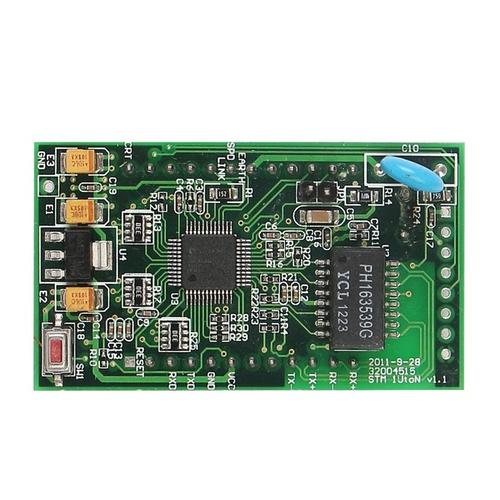
At this time, PCB has two main functions. One is to etch the interconnected circuit graph on the copper-covered layer, avoiding the need for a lot of manual welding line operations. Only manual placement of components and device pin welding and fixing can be done, which greatly improves production efficiency and reliability. The second function of PCB is to serve as the support and fixing carrier of components. In the 1950s, components were all in-line packages with pins, so if components were to be installed on PCB, corresponding holes must be drilled out on PCB. Therefore, in addition to copper interconnection pattern, PCB must also have holes. In the 1950s, PCB only had a single panel with a single side covered with copper foil. Because the metallization technology of the holes had not been developed, the holes on PCB were metallized at that time (that is, the holes did not realize the internal interconnection). However, with the improvement of the packaging technology of electronic components, the volume became smaller and smaller. More and more electronic components are installed on the same board to achieve more complex functions. As the wiring density of PCB increases, the problem of crossing wires appears. A single panel only has one wiring layer, so the wiring space is naturally insufficient. Metal leads are then threaded from the other side of the PCB as jumpers to achieve interconnection).
Electronic circuits are always developing towards more and more complex functions and higher wiring density. Engineers have to start to consider how to realize the two sides of the PCB enough wiring, which needs to solve the interconnection problem. Wire layering must be perforated, and then the interconnection of different wiring layers can be realized through this hole. Now we know that metalizing interconnection can be realized through electroplating to sink copper through the hole wall. At present, electroplating is also the mainstream process of plate factory, but in the early 1950s, this method has not been developed. Or now, if you want to DIY Double Layer PCB at home or in the laboratory, how to achieve through hole interconnection without electroplating metallization technology?
Two methods are commonly used.
The first is the threading method, that is, in the need to change the end of the line at the end of the pad, drill a hole in the pad, and then use metal wire through the hole, and finally through the hole at both ends of the pad metal wire welding fixed, of course, can also directly use the pin of the device to achieve the interconnection of different layers.
Another method is the interconnection method using hollow rivets.
There are also more recent approaches, such as chemical-free through-hole metallization similar to the German LPKF.
When it comes to DIY double panels, it was still quite expensive for students to make a double-sided PCB circuit board at that time, the delivery time was six or seven days, and the logistics was not as developed as now. Therefore, DIY was still chosen for simple circuit boards, which was to etch copper coated plates with ferric chloride to make interconnected circuits.
DIY single panel is not difficult, at most is some broken line or etched incomplete line needs to be manually repaired, but DIY double panel is much more painful, first in the circuit diagram exposure link to pay attention to different layers of hole position, and then is to realize the interconnection of holes, this is the most time-consuming is also the most painful link, even if only dozens of holes, drilling, After threading thin wires through the holes, and finally welding them together, it takes a lot of work, dizziness and neck pain.
If you use a special rivet crimp, then a slightly easier way to use hollow rivet crimp method, as shown in the above video, but the material cost is much more expensive than fine wire, the biggest problem is that the hole can not be made too small, the smallest rivet diameter is 0.4mm, but this is foreign, domestic treasure on the minimum diameter is 1mm, So the hole and hole ring should be made larger, which also reduces the wiring density.
Words no rotten circuit board of electronic engineers life is not complete, but only need to experience the method is good, life is short, timely Jialichuang is the king picture
Even the use of special crimping tools to crib hollow rivets to achieve the interconnection of dual panels was not a cost and efficiency optimization method, and the connection was not reliable enough. Engineers had to continue to study, until 1953, the American MOTOROLA company released the electroplating through hole metallization method, which made dual panels popular.

On April 19, 1965, Gordon Moore, then an engineer at Fairchild Semiconductor, published a prediction in Electronics Magazine that the number of transistors and resistors integrated on semiconductor chips would double each year. With the appearance of IC (Integrated Circuit) and LSI (Large Scale Integration), electronic equipment is also developing towards the direction of thinner and shorter, at the same time, the number of IC pins and peripheral electronic components increases sharply, making the wiring density increase. Dual panels are no longer sufficient, which has led to the development of multi-layer PCB technology.
In order to achieve high density interconnection, increasing the number of PCB wiring layers is one direction, reducing the line width/line distance of the wiring and reducing the diameter of the drill hole is also one direction to improve the wiring density.
Of course, mechanical drilling depends on the drill, the smaller the drill can be made, the smaller the drill can be processed, but the physical specifications of the drill can not be reduced without limitation, the hole diameter is less than 0.2mm, and the ratio of the hole diameter to the PCB thickness exceeds a certain limit, mechanical drilling and subsequent metallization plating will face great challenges.
In the 1980s, with the development of VLSI (Very large-scale integration), the application of multi-layer printed circuit board has been developed rapidly, and the wiring density has also increased sharply. In order to meet the challenges of high-density wiring, interlayer interconnection technology has also been developed accordingly. For example, there are laser drilling, blind hole, buried hole, plate hole and so on HDI process.
Hole classification and its function on PCB
Feb 04,2023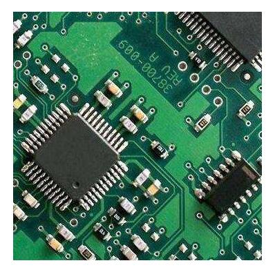


Just upload Gerber files, BOM files and design files, and the KINGFORD team will provide a complete quotation within 24h.