
Professional PCB manufacturing and assembly
Building 6, Zone 3, Yuekang Road,Bao'an District, Shenzhen, China
+86-13410863085Mon.-Sat.08:00-20:00

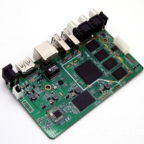
Printed circuit board is one of the important parts of electronic industry, which is the carrier of the connection between various electronic components in electronic products. This article will share common PCB circuit board defect detection techniques, hoping to be helpful to users.
The common defect detection technology of PCB circuit board includes automatic optical detection technology, machine vision detection technology, computer vision detection technology and so on.
1. Manual visual subjective decision method
Operators need to use electron microscope or magnifying glass to determine the qualified rate of PCB board according to their subjective experience and visual measurement. This technology has a low budget and cost, and the equipment required is cheap and easy to operate. However, the accuracy is low, the efficiency of defect detection is low, and the data set analysis is difficult.
2. Instrument online detection method
Through simulation test and electrical performance test, operators can check the circuit board welding faults such as open circuit and short circuit and the functional detection of components. They can also detect the electronic components with excessive density on circuit board by boundary scanning technology. The collective detection of circuit board welding points and connections is a detection technology based on electrical signals as the medium. This technology has the advantages of high conversion rate, low cost, large detection coverage, but difficult operation, long operation time.
3. Functional testing method
Operators use special testing equipment to fully test the functional modules of the circuit board in the production line, so as to confirm the status of the circuit board. However, depth data such as improved electronic components and pin diagnosis cannot be provided, so different testing equipment should be used according to different requirements, which makes it difficult to write programs.
4. Visual detection technology
Visual detection technology has covered many fields such as electronics, computer, artificial intelligence, image processing, etc., and has become the mainstream PCB defect detection research method in today's society. It is mainly divided into:

(1) Automatic Optical Detection Technology (AOI) :
The welding defects of PCB were detected and processed based on optical principle by integrating various computer technologies such as image processing and automatic control. The image of PCB solder spot area is obtained by scanning PCB with camera, and PCB defects are detected automatically by visual processing technology. Characteristic data of each solder spot is extracted and compared with database to determine and identify the defect type of solder spot, and the number of detection results is given.
(2) Machine vision detection technology (MVI) :
Combined with CMOS, digital image sensor, DSP, FPGA and other technologies, the use of machines instead of naked eyes for a variety of PCB measurement and judgment, because of the use of a variety of machine technology, in the field of precision testing is popular, often used in industrial PCB board detection, with fast speed, non-contact, good flexibility advantages, easy to avoid huge losses in PCB production line. It has high economic value.
(3) Computer Vision detection Technology (AVI) :
The technology is based on computer vision research and development, is a new high-tech industrial detection technology, through the image sensor to achieve three-dimensional measurement of the size and spatial position of the measured object, the data obtained in the computer and fault image data for comparison or extraction, and according to the detection parameters to guide the electronic equipment action, with high aging, strong resistance and other characteristics


Just upload Gerber files, BOM files and design files, and the KINGFORD team will provide a complete quotation within 24h.