
Professional PCB manufacturing and assembly
Building 6, Zone 3, Yuekang Road,Bao'an District, Shenzhen, China
+86-13410863085Mon.-Sat.08:00-20:00

SMT principle and poor PCB data lead to possible results
Principle Surface Mount System
Different types of mounters have their own advantages and disadvantages, which usually depends on the application or technology of the system. There is a trade-off between speed and accuracy. In wafer placement technology, the component placement process of any wafer placement machine includes PCB transmission, component picking, support and identification, inspection and adjustment, component placement and other steps.
1. PCB transmission
PCB transmission is the first step to install components on the smt mounter. This is a process of accurately guiding the PCB components to be bonded to the designated position of the assembly machine mainly through the transmission mechanism. After that, the PCB transmission system needs stable PCB output and components.
2 PCB reference calibration standard
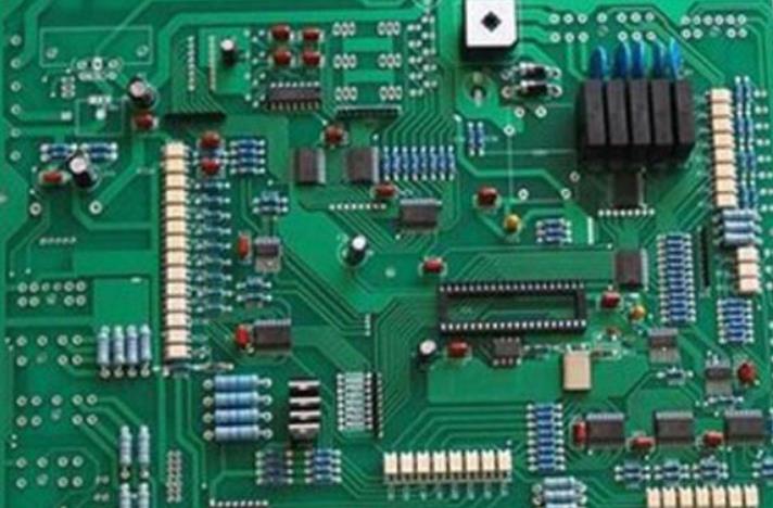
Circuit board

When the smt machine is running, the upper corner of the PCB (usually the lower left corner and the upper right corner) is used as the origin for calculating the component mounting coordinates. Some errors may occur during PCB processing. In this case, PCB must be placed during high-precision assembly.
3. Collect components
Component collection refers to the collection of wafer components from packages. In this process, the key is the accuracy and correctness of the collection. Factors that affect this process include collection tools and methods, component packaging methods, and relevant characteristics of the component itself.
There are two collection methods, manual collection and machine collection. The machine selection includes two modes: mechanical clamping and vacuum suction. Machine picking tools are more complex than manual picking. Almost all modern SMT machines use vacuum pumping. Only under special circumstances, such as some large and special shaped parts, can they be installed by mechanical clamping.
4. Detection and adjustment
After the core arranging machine absorbs the components, two problems need to be determined: whether the center of the first component is consistent with the center of the installation head. If the center of the module is not consistent with the center of the installation head, and no adjustment is made, the final deviation of the module will be caused;
If the second component meets the installation requirements, the second component cannot be installed. These two problems must be determined by testing.
Bad PCB data leads to 6 possible results
1. The heat resistance and thermal expansion characteristics of the substrate do not match the component design, solder, welding process and temperature, resulting in PCB deformation/deformation and serious welding defects.
2. The change of the substrate welding coating material or its heat resistance and welding resistance do not match with the welding, and the high temperature during the welding process leads to poor wettability or excessive wettability and low weldability.
3. The weldable lining or weldable strength data do not meet the application requirements of relevant processes, resulting in plate corrosion.
4. The PCB solder coating process is out of control, the copper foil surface is seriously oxidized or polluted, the characteristics of the solder coating materials are different, or their heat resistance and solder resistance are inconsistent with the welding temperature and welding process, resulting in copper exposure on the bonding pad.
5. If resistance welding or resistance welding is not carried out, the wiring spacing of wires is too small, PCB wiring will exceed the tolerance, resulting in wire welding.
6. The heat resistance of the base plate is poor, and the laminating process and data quality are not controlled, resulting in PCBA lamination and foam


Just upload Gerber files, BOM files and design files, and the KINGFORD team will provide a complete quotation within 24h.