
Professional PCB manufacturing and assembly
Building 6, Zone 3, Yuekang Road,Bao'an District, Shenzhen, China
+86-13410863085Mon.-Sat.08:00-20:00

Inspection of SMT machining surface assembly process
The quality and reliability of surface mount products mainly depend on the manufacturability and reliability of components, electronic process data, process design and assembly process In order to successfully assemble PCB products, on the one hand, the quality of electronic components and process data needs to be strictly controlled, that is, incoming inspection; On the other hand, the assembly process must be reviewed for the manufacturability (DFM) of the SMT process design Before and after each process in the implementation process, process quality inspection shall also be carried out, that is, surface assembly process inspection, including the quality inspection methods and strategies, repair, and welding of each process in the entire assembly process (such as printing)
1) Content of Solder Paste Printing Process Inspection
Solder paste printing is the initial step in SMT process. This is the most complex and unstable process. It is affected by many factors and has dynamic changes. It is also the source of most defects. 60% - 70% defects occur. In the printing stage. If an inspection station is set up after printing to inspect the printing quality of solder paste in real time and eliminate the defects in the initial link of the production line, the loss and cost can be minimized. In this regard, more and more SMT production lines are equipped with automatic optical detection for the printing process, and even some printers have integrated solder paste printing systems, such as AOI. Common printing defects during solder paste printing include non rotating solder, excessive solder, solder paste scratch in the middle of large solder pads, solder paste sharpening at the edge of small solder pads, printing offset, bridging and pollution. The reasons for waiting for these defects include poor liquidity of solder paste, improper processing of template thickness and hole wall, unreasonable printer parameter setting, insufficient precision, improper selection of blade data and hardness, and poor PCB processing.
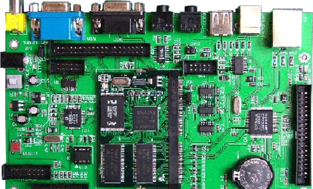
SMT processing factory 6
Circuit board

2) Inspection contents during component placement
The placement process is SMT production line It is one of the key factors to determine the degree of automation, the assembly accuracy and productivity of the assembly system It has a decisive influence on the quality of electronic products Therefore, real-time monitoring of the placement process is of great significance to improve the quality of the entire product The inspection flow chart before the furniture (after placement) is shown in Figure 6-3. The most basic method is to add AOI after the high-speed placement machine and before reflow soldering to check the placement quality On the one hand, it can prevent defective solder paste printing and placement from entering the reflow stage, thus bringing more on the other hand. It provides support for timely proofreading and maintenance of the mounter, so that it is always in good working condition The inspection contents during placement mainly include the placement accuracy of components, the control of fine pitch devices and BGA placement, various defects before reflow soldering, such as lack of components, offset, solder paste collapse and offset, PCB board surface contamination, pins not contacting with solder paste, etc Use the character recognition software to read the value and polarity recognition of components, and determine whether the pasting is wrong or reversed
3) Welding process inspection content
Inspection after welding requires 100% inspection of products. Generally, the following items need to be checked: check whether the surface of the solder joint is smooth, whether there are holes, holes, etc.; Check whether the solder joint shape is half moon shaped and whether there is more or less tin; Check whether there are tombstones, bridges, component displacement, component missing, tin beads and other defects; Check all components for polarity defects; Check whether the welding has short circuit, open circuit and other defects; Check the color change of PCB surface.
The above is the explanation given by the editor of pcb circuit board company.
If you want to know more about PCBA, you can go to our company's home page to learn about it.
In addition, our company also sells various circuit boards,
High frequency circuit board and SMT chip are waiting for your presence again.


Just upload Gerber files, BOM files and design files, and the KINGFORD team will provide a complete quotation within 24h.