
Professional PCB manufacturing and assembly
Building 6, Zone 3, Yuekang Road,Bao'an District, Shenzhen, China
+86-13410863085Mon.-Sat.08:00-20:00


What are the methods of PCBA double-sided reflow soldering?
Double side reflow soldering method One side of polychlorinated biphenyl SMT process workshop adopts red glue process, and the other side adopts solder paste process of SMT process equipment This method is applicable to PCB boards with dense electronic components and different component heights and sizes on one side In particular, the gravity of large electronic components is very high, and then they fall off after reflow soldering in the SMT technology production workshop At this time, the red glue will be stronger when heated
The process flow of red glue is as follows: 1. Incoming inspection II. Screen printed solder paste on side a of the printed circuit board 3. Patch 4. AOI or QC check 5. A Reflow soldering on side 6. Turnover 7. Screen printing red glue or red glue on the B side of the printed circuit board (note whether red glue or red glue is used to apply the red glue to the middle part of the component, and the red glue must not contaminate the bonding pad, making the component pins cannot be welded)>Repair>Drying>Cleaning>Testing>Repair.
Reflux launder

Here, PCBs should be welded on the solder paste surface before drying the red glue surface Because the drying temperature of red glue is relatively low, it can be cured at about 180 degrees If the red glue surface is dried first and then the solder paste surface is operated, it is easy to cause PCBs of electronic components to fall off After all, the adhesive force of red glue is not as good as that of tin. When passing through the solder paste plate, the temperature should be above 200 degrees, which easily makes the solidified red glue brittle and causes a large number of components to fall off
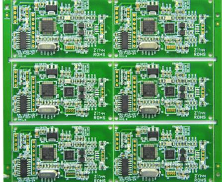
Solder paste process is adopted on both sides of PCBs. This method is applicable to many components on both sides, and both sides of the PCB board have large density pin IC or BGA PCB boards. Because if you use red glue, it is easy to misplace IC pins and pads.
The solder paste process flow is as follows: the first incoming inspection of the patch processing plant>screen printed solder paste on the a side of PCB>patch>QC or AOI inspection>reflow soldering on the a side>turnover>screen printed solder paste on the B side of PCB>patch>QC or AOI inspection>reflow soldering>cleaning>inspection>repair. It should also be noted here that in order to prevent large components from falling off when passing through the B surface of PCB, SMT technology operators should set the temperature of the fusion area in the lower temperature area of reflow soldering to be slightly lower than the temperature in the higher temperature area of reflow soldering when setting the reflow soldering temperature. In this way, the tin below will not melt again, causing the parts to fall off.
The above is the explanation given by the editor of pcb circuit board company.
If you want to know more about PCBA, you can go to our company's home page to learn about it.
In addition, our company also sells various circuit boards,
High frequency circuit board and SMT chip are waiting for your presence again.


Just upload Gerber files, BOM files and design files, and the KINGFORD team will provide a complete quotation within 24h.