
Professional PCB manufacturing and assembly
Building 6, Zone 3, Yuekang Road,Bao'an District, Shenzhen, China
+86-13410863085Mon.-Sat.08:00-20:00

The knowledge of plate assembly that PCB processing industry has to know
PCB manufacturing, PCB design and PCBA processing manufacturers will explain to you the knowledge of plate assembly that PCB processing industry has to know
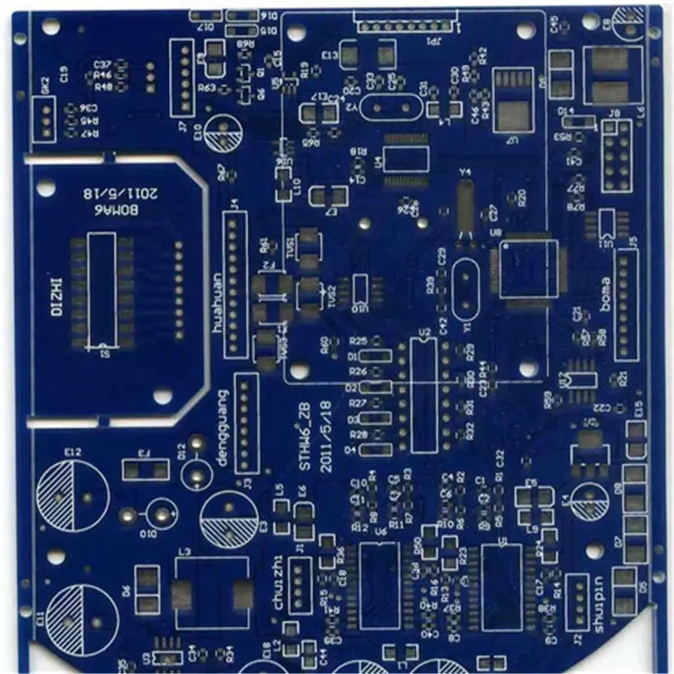
Except for the large single circuit boards that cannot be spliced, PCB assembly is usually the shipping method of circuit board manufacturers. However, the specific parameters such as PCB assembly mode and number need to be determined by comprehensively considering various factors when PCB production is completed and delivered. Since the original raw material of FR4 is a square standard plate, it will cause huge waste if it is cut directly instead of splicing. The main purpose of panel splicing is to save production time, produce materials and make more effective use of machinery and equipment, effectively use the area of panels, and reduce unnecessary cost waste.
The outer frame of the PCB panel should also be carefully considered to ensure that the PCB will not deform after being fixed on the fixture. Generally, it is not allowed to open a V slot on the outer frame of the PCB. For the layout of components, it is necessary to ensure that all orientations are consistent, and there should be no such situations as mirror images that affect the V-cutting process, which will cause problems in the coordinate positioning of processing and can not accurately assemble boards. There shall be no connector between the outer frame of the panel and the inner small board, or between the small board and the small board. If this situation exists, it will prevent the tool from separating the boards after welding. In order to ensure the position and level of the detection board, we need to set more than three positioning points on the edge of the board. Through optical detection of these three points, we can obtain the reference coordinates of the whole panel processing and the levelness of PCB.
How many unit boards should be included in a panel? What I want to tell you is that the number problem is determined by the PCB design engineer according to the actual situation of each PCB. In principle, the more the number is, the better. The more the number is, the less the transmission loss time of a single PCB on the track is, and the higher the utilization rate of equipment is; At the same time, the greater the number of panels, the higher the utilization rate of materials used in PCB manufacturing, and the lower the cost. However, there is a limit to the number of panels. With the increase of the number of PCBs, the material cost of unit boards may rise, mainly because the equipment capacity of PCB manufacturers is limited. Our common methods are ABAB or AAAA. The density and distribution of electronic components on the PCB board as well as the equipment configuration should be considered to determine which way to use for panel assembly. Therefore, each panel assembly method has its advantages and disadvantages.
PCB manufacturing, PCB design and PCBA processing manufacturers will explain to you the knowledge of plate assembly that PCB processing industry has to know.


Just upload Gerber files, BOM files and design files, and the KINGFORD team will provide a complete quotation within 24h.