
Professional PCB manufacturing and assembly
Building 6, Zone 3, Yuekang Road,Bao'an District, Shenzhen, China
+86-13410863085Mon.-Sat.08:00-20:00

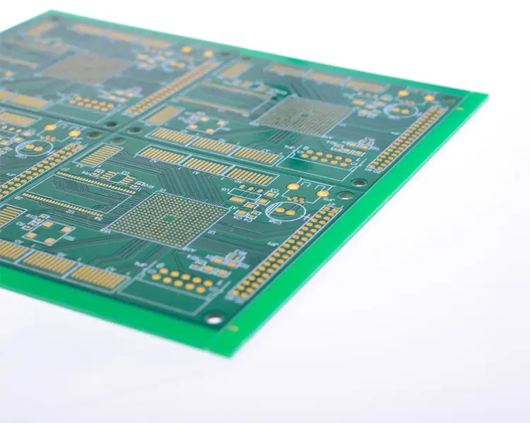
PCB proofing refers to the trial production of printed circuit boards before mass production. It is mainly used in the process of small batch trial production to the factory after electronic engineers have designed circuits and completed PCBs. This process belongs to what we understand as "" before the product design is confirmed and tested.
Pcb proofing
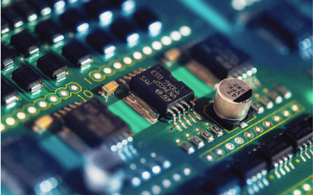
PCB proofing surface treatment generally adopts hot air leveling and tin spraying, full board nickel gold plating, organic solderability protector (OSP), silver deposition
, gold precipitation, tin precipitation, hard gold electroplating, chemical nickel palladium and other processes to ensure good solderability or electrical performance, and these processes need to fully consider the production strength and service level of service providers.
As a professional and PCB manufacturing factory, Fanyi PCB, based on the technology of Silicon Valley in the United States, is specialized in high-speed and high-density PCB product services. It uses advanced cutting-edge production processes and high-quality raw materials, strictly standardizes operation standards and incoming and outgoing QC standards, ensures that the shipped products reach the precision quality, and provides customers with one-stop comprehensive services for rapid proofing and production of medium and high difficulty PCB circuit boards.
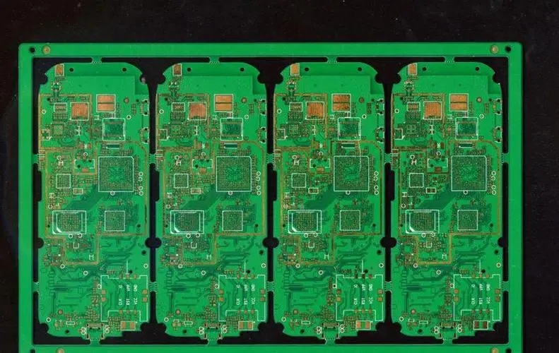
PCB differentiation between HDI board and blind hole board
HDI is a product of circuit board, which is called highDensityInterconnection. At present, high-order electronic products are generally products of high-density interconnection boards.
Blindvias: Blind holes are vias that connect the inner layer routing of a PCB with the surface layer routing of a PCB. This hole does not penetrate the entire board.
Buried vias: Buried vias only connect the via type of wiring between inner layers, so they cannot be seen from the PCB surface.
With the development of portable product design towards miniaturization and high density, it is more and more difficult, which puts forward higher requirements for PCB production process. At present, most portable products use the design process of BGA packaging with a spacing of less than 0.65mm. What is the blind buried hole?
Blindvias: Blindvias are vias that connect PCB inner layer routing with PCB surface layer routing. This hole does not penetrate the whole board.
Buried vias: Buried vias only connect the via type of wiring between inner layers, so they cannot be seen from the PCB surface.
The circuit board with buried blind holes is not necessarily HDI circuit board, but generally HDI boards have blind holes, so the buried holes are not necessarily. It depends on the level and pressure of your circuit board product.
Blind buried orifice plate
The description is as follows:
The first and second order of 6-layer circuit boards are for boards that need laser drilling, namely HDI boards
First order HDI board of 6-layer circuit board refers to blind holes: 1-2,2-5,5-6. That is, 1-2,5-6 needs laser drilling
Second order HDI board of 6-layer circuit board refers to blind holes: 1-2,2-3, 3-4, 4-5, 5-6. That is, two laser drilling is required
First drill 3-4 buried holes, then press 2-5, then drill 2-3, 4-5 laser holes for the first time, then press 1-6 for the second time, then drill 1-2, 5-6 laser holes for the second time, and finally drill through the hole. It can be seen that the second order HDI plate has been pressed twice and laser drilled twice
In addition, the second order HDI board is also divided into staggered hole second order HDI board and stacked hole second order HDI board. The staggered hole second order HDI board means that the blind holes 1-2 and 2-3 are staggered, while the stacked hole second order HDI board means that the blind holes 1-2 and 2-3 are stacked together, for example: blind: 1-3, 3-4, 4-6


Just upload Gerber files, BOM files and design files, and the KINGFORD team will provide a complete quotation within 24h.