
Professional PCB manufacturing and assembly
Building 6, Zone 3, Yuekang Road,Bao'an District, Shenzhen, China
+86-13410863085Mon.-Sat.08:00-20:00

Introduction to Horizontal Plating Process by PCB Manufacturer
With the rapid development of microelectronics technology, the manufacturing of printed circuit boards is developing towards multilayer, lamination, functionality and integration, which makes the manufacturing technology of printed circuit boards more difficult. The conventional vertical electroplating process cannot meet the technical requirements of high-quality and high reliability interconnection holes, so horizontal electroplating technology is generated. This paper analyzes and evaluates the horizontal electroplating technology from the principle of horizontal electroplating, the basic structure of horizontal electroplating system, and the development advantages of horizontal electroplating. It points out that the use of horizontal electroplating system is a great development and progress for the printed circuit industry. The following is a detailed explanation of the horizontal electroplating process of high-precision PCB:
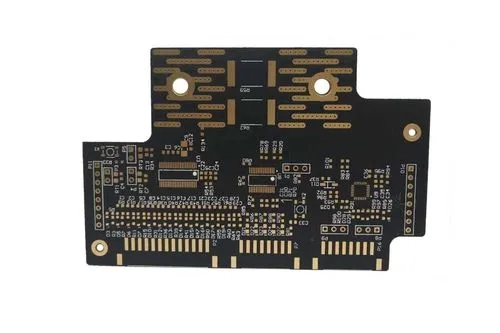
PCB horizontal electroplating machine
summary
With the rapid development of microelectronics technology, the manufacturing of printed circuit boards is developing rapidly in the direction of multi-layer, multilayer, functional and integrated. It urges the printed circuit design to adopt a large number of tiny holes, narrow spacing, and thin wires for the conception and design of circuit graphics, which makes the manufacturing technology of printed circuit boards more difficult. Especially, the aspect ratio of through holes in multilayer boards exceeds 5:1, and the large number of deep blind holes used in multilayer boards make the normal vertical electroplating process unable to meet the technical requirements of high-quality and highly reliable interconnection holes.
The main reason is to analyze the current distribution state from the electroplating principle. Through actual electroplating, it is found that the current distribution in the hole presents a waist drum shape. The current distribution in the hole gradually decreases from the hole edge to the hole center, resulting in a large amount of copper deposition on the surface and the hole edge. It is impossible to ensure the standard thickness of the copper layer at the part where copper is required in the hole center. Sometimes the copper layer is extremely thin or there is no copper layer, which may cause irreparable loss in serious cases, A large number of multilayer boards were scrapped.
In order to solve the product quality problem in mass production, the current and additives are used to solve the deep hole electroplating problem. In the copper electroplating process for high aspect ratio printed circuit boards, most of them are carried out under relatively low current density with the assistance of high-quality additives, moderate air agitation and cathode movement. The effect of electroplating additives can be shown only when the electrode reaction control area in the hole is enlarged. In addition, the cathode movement is very conducive to the improvement of the deep plating ability of the plating solution. The polarization of the plating piece is increased, and the formation speed of crystal nucleus and the growth speed of crystal grains in the electrodeposition process of the coating are mutually compensated, thus obtaining a high toughness copper layer.
However, when the aspect ratio of the through-hole continues to increase or deep blind holes appear, these two process measures are weak, so horizontal electroplating technology is generated. It is a continuation of the development of vertical electroplating technology, that is, a novel electroplating technology developed on the basis of vertical electroplating technology. The key of this technology is to manufacture an appropriate and mutually supporting horizontal electroplating system, which can enable the plating solution with high dispersion capacity to show more excellent functions than the vertical electroplating method with the cooperation of improved power supply mode and other auxiliary devices.
PCB manufacturers, PCB designers and PCBA processors will explain the horizontal electroplating process of PCB PCB.
Do you know the production of blind hole board?
Nov 10,2022


Just upload Gerber files, BOM files and design files, and the KINGFORD team will provide a complete quotation within 24h.