
Professional PCB manufacturing and assembly
Building 6, Zone 3, Yuekang Road,Bao'an District, Shenzhen, China
+86-13410863085Mon.-Sat.08:00-20:00

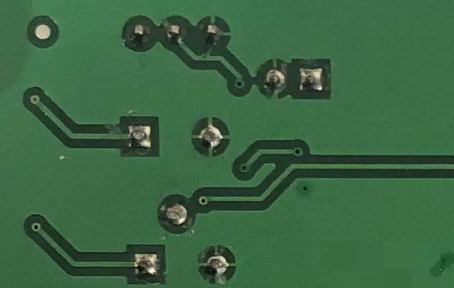
FPC chemicalnickel gold is a popular term, and the correct term should be called nickel leaching gold (EN/IG) No additional current is required for the formation of chemical nickel layer. With the action of reducing agent (such as sodium dihydrogen hypophosphite NaH2PO2, etc.) in the bath solution, continuous deposition of nickel phosphorus alloy layer can be carried out on the activated metal surface to be plated at high temperature. The chemical nickel layer can be used as a shielding layer for metal atom migration to prevent copper from diffusing to the gold coating
FPC
As for gold dipping, it is a typical displacement reaction without reductant When the chemical nickel surface enters the gold leaching bath, the gold layer is deposited on the nickel metal at the same time as the nickel layer is dissolved and thrown away Once the nickel surface is completely covered by the gold layer, the deposition reaction of the gold layer gradually stops and it is difficult to increase to a certain thickness As for another series of thickened gold, strong reducing agent is needed to gradually thicken the gold layer
Nickel alloy has been widely used for its solderability and can also provide a substrate for IC chip bonding (Au/Al wire)
In fact, the welding strength of solder joints formed by plated nickel gold to PCB parts is almost all built on the surface of nickel layer. The purpose of gold plating is to protect the nickel surface from passivation or oxidation in the air, and maintain the minimum solderability The gold layer itself is completely unsuitable for PCB welding, and its solder joint strength is also very poor
At the moment of high temperature welding of circuit boards, gold and tin have already formed different forms of interface alloy compounds (such as AuSn, AuSn2, AuSn4, etc.) and escaped. Therefore, the real basis of solder joints are all landed on the nickel surface, and the strength of solder joints has nothing to do with gold That is to say, the tin in the solder will form Ni3Sn4 interface alloy eutectic with pure nickel The thin gold layer will disperse quickly in a short time and slip into a large amount of solder, so the gold layer can not form reliable PCB solder joints at all
5 Principles of FPC Production
FPC
In the process of FPC, in order to save costs, improve production efficiency and shorten production cycle, it will be produced in the form of patchwork rather than monolithic production. There are several principles to follow when assembling FPC.
1. On the premise that each process can be produced, try to "squeeze" the plate. The so-called "extrusion" is to reduce the distance between adjacent plates, so as to reduce the size of the whole plate assembly, save production materials and reduce production costs.
2. The spacing between single plates shall be at least 2.5mm. First of all, this is to meet the requirements for positioning holes. In the process of mass production, die stamping is generally used for molding. In order to enhance the accuracy of die stamping, positioning holes need to be placed between each piece in the assembly to avoid the offset of die stamping, which will lead to the scrapping of FPC; In the process of sample production, laser cutting is generally used for forming. In order to avoid slight deviation and avoid deviation of one piece and the whole piece, single pieces cannot be directly connected, so that they do not affect each other.
3. Etched characters shall be added to the plate assembly, and the size and quantity of the plate assembly shall be briefly described, so as to facilitate the check and verification in subsequent production.
4. Add positioning holes at the four corners of the whole assembly, and select one corner to mark different positioning holes, so as to keep the direction consistent in the subsequent process production, so as not to lead to the return of film sealing and character printing.
5. The width of the plate shall be fixed as 250mm and the length shall be within 250mm as far as possible. The larger the size of the plate, the greater the offset, the worse the production precision, and the higher the defective rate of finished products.
After knowing the five principles that need to be followed, I will briefly introduce the three ways of composition.
1. Regular composition. The pattern is directly arranged in the direction of a single piece, which is most suitable for FPC pattern with regular shape, such as rectangle, square, circle, ellipse, etc;
2. Oblique splicing. Tilt the single piece to a certain extent, and then array it, so as to maximize the use of the space for the assembly, such as the curved bars, folds, etc;
3. Reverse stitching. That is, combine one positive and one negative of a single PCS.
See why the 32 layer PCB proofing is expensive
Nov 09,2022


Just upload Gerber files, BOM files and design files, and the KINGFORD team will provide a complete quotation within 24h.